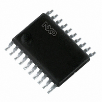
74LVC541APW,112 NXP Semiconductors, 74LVC541APW,112 Datasheet - Page 10

74LVC541APW,112
Manufacturer Part Number
74LVC541APW,112
Description
IC BUFF/DVR TRI-ST 8BIT 20TSSOP
Manufacturer
NXP Semiconductors
Series
74LVCr
Datasheet
1.74LVC541AD118.pdf
(17 pages)
Specifications of 74LVC541APW,112
Logic Type
Buffer/Line Driver, Non-Inverting
Package / Case
20-TSSOP
Number Of Elements
1
Number Of Bits Per Element
8
Current - Output High, Low
24mA, 24mA
Voltage - Supply
2.7 V ~ 3.6 V
Operating Temperature
-40°C ~ 125°C
Mounting Type
Surface Mount
Logic Family
74LVC
Number Of Channels Per Chip
8
Polarity
Non-Inverting
Supply Voltage (max)
3.6 V
Supply Voltage (min)
1.2 V
Maximum Operating Temperature
125 C
Mounting Style
SMD/SMT
High Level Output Current
- 24 mA
Input Bias Current (max)
40 uA
Low Level Output Current
24 mA
Maximum Power Dissipation
500 mW
Minimum Operating Temperature
- 40 C
Output Type
3-State
Propagation Delay Time
6.5 ns
Number Of Lines (input / Output)
8 / 8
Lead Free Status / RoHS Status
Lead free / RoHS Compliant
Lead Free Status / RoHS Status
Lead free / RoHS Compliant, Lead free / RoHS Compliant
Other names
568-1587-5
74LVC541APW
935260903112
74LVC541APW
935260903112
Philips Semiconductors
AC WAVEFORMS
2003 Nov 12
handbook, full pagewidth
Octal buffer/line driver with 5 V
tolerant inputs/outputs (3-state)
1.2 V
2.7 V
3.0 to 3.6 V
1.2 V
2.7 V
3.0 to 3.6 V
V
V
CC
CC
0.5
1.5 V
1.5 V
0.5
1.5 V
1.5 V
V
V
V
V
M
HIGH-to-OFF
M
OFF-to-HIGH
CC
LOW-to-OFF
OFF-to-LOW
CC
OEn input
output
output
handbook, halfpage
Fig.6 Input (An) to output (YN) propagation delays.
V
2.7 V
2.7 V
V
2.7 V
2.7 V
Yn output
An input
CC
CC
GND
GND
V OH
V CC
V OL
Fig.7 3-state enable and disable times.
V
V I
V
I
I
INPUT
INPUT
GND
V OH
V OL
V I
enabled
V M
outputs
2.5 ns
2.5 ns
2.5 ns
2.5 ns
2.5 ns
2.5 ns
t PLZ
t
t
t PHZ
r
r
= t
= t
f
f
V M
V X
10
V Y
V M
t PHL
V
output load.
V
V
V
V
V
output load.
OL
X
X
Y
Y
OL
disabled
outputs
= V
= V
= V
= V
and V
and V
OL
OL
OH
OH
+ 0.3 V at V
+ 0.1 V at V
OH
OH
0.3 V at V
0.1 V at V
t PZL
t PZH
are typical output voltage drop that occur with the
are typical output voltage drop that occur with the
MNA901
t PLH
V M
CC
CC
CC
CC
V M
< 2.7 V;
< 2.7 V.
2.7 V;
enabled
2.7 V;
outputs
MNA902
Product specification
74LVC541A


