TDA9983BHW/8/C1,55 NXP Semiconductors, TDA9983BHW/8/C1,55 Datasheet
TDA9983BHW/8/C1,55
Specifications of TDA9983BHW/8/C1,55
Available stocks


Related parts for TDA9983BHW/8/C1,55


TDA9983BHW/8/C1,55 Summary of contents
Page 1
TDA9984A HDMI 1.3 transmitter with 1080p upscaler embedded Rev. 04 — 15 January 2009 1. General description The TDA9984A is a High-Definition Multimedia Interface (HDMI) v. 1.3 transmitter with embedded 1080p upscaling functionality backward compatible DVI 1.0 and ...
Page 2
... NXP Semiconductors I Programmable color space converter allows to input RGB video data and to output RGB or YCbCr HDMI video data input YCbCr video data and to output RGB or YCbCr HDMI video data; converter can be passed I Upscaler allows creating a 1080p output from a standard definition input by using ...
Page 3
... NXP Semiconductors 4. Quick reference data Table 1. Quick reference data DD(3V3) DD(1V8) Typical values are measured at T Symbol Parameter V programming voltage PP V free running oscillator analog supply DDA(FRO)(3V3) voltage (3 PLL analog supply voltage (3.3 V) DDA(PLL)(3V3) V digital supply voltage (3.3 V) ...
Page 4
DDD(3V3) PP DDC(1V8) DDH(3V3) 3 13, 48, 71 59 AP0 to AP7 AUDIO CONTENT AUDIO FIFO AUDIO AUDIO INFO-FRAME PROCESSING 12 CTS/N ACLK ACR VIDEO INFO-FRAME OTHER ...
Page 5
... NXP Semiconductors 7. Pinning information HSYNC/HREF 1 2 VSYNC/VREF AP7 4 AP6 5 6 AP5 AP4 7 AP3 8 9 AP2 10 AP1 AP0 11 ACLK DDD(3V3 SSD V 15 SSA(PLL)(1V8 DDA(PLL)(1V8) 17 INT HPD 18 DDC_SDA 19 20 DDC_SCL Fig 2. Pin configuration 7.1 Pin description Table 3. Symbol HSYNC/HREF VSYNC/VREF ...
Page 6
... NXP Semiconductors Table 3. Symbol AP2 AP1 AP0 ACLK V DDD(3V3) V SSD V SSA(PLL)(1V8) V DDA(PLL)(1V8) INT HPD DDC_SDA DDC_SCL TM V SSA(FRO)(3V3) V DDA(FRO)(3V3) EXT_SWING V SSH TXC TXC+ V DDH(3V3) TX0 TX0+ V SSH TX1 TX1+ V DDH(3V3) TX2 TX2+ V SSH V DDA(PLL)(3V3) V SSA(PLL)(3V3) ...
Page 7
... NXP Semiconductors Table 3. Symbol V DDD(3V3) VPC[7] VPC[6] VPC[5] VPC[4] VPC[3] VPC[2] VPC[1] VPC[0] VPB[7] VPB[6] V DDC(1V8) V SSC VPB[5] VPB[4] VPB[3] VPB[2] VPB[1] VCLK VPB[0] VPA[7] VPA[6] VPA[5] V DDD(3V3) V SSD V SSC V DDC(1V8) VPA[4] VPA[3] VPA[2] VPA[1] VPA[0] DE/FREF [ Power supply Ground Input Output. ...
Page 8
... NXP Semiconductors 8. Functional description The TDA9984A is designed to convert digital data (video and audio) provided by a Set-Top Box or DVD into an HDMI output, which could be used in TV with HDMI or DVI input. The TDA9984A is able to output HDMI with the formats: • RGB • YCbCr • ...
Page 9
... NXP Semiconductors The device can swap and invert (in case of a little endian stream) the incoming video data via the I to match the expectation of the video processing block; see When input ports are not used possible to map them to internal ground via the ...
Page 10
Table 5. Inputs of video input formatter Space color Format Channels Sync RGB 8-bit external embedded YCbCr 8-bit external embedded YCbCr ...
Page 11
... NXP Semiconductors 8.1.2.1 RGB external sync input (rising edge) Table 6. RGB mapping Register VIP_CNTRL_0 = 23h; VIP_CNTRL_1 = 45h; VIP_CNTRL_2 = 01h. Video port A Video port B Pin RGB Pin VPA[0] B[0] VPB[0] VPA[1] B[1] VPB[1] VPA[2] B[2] VPB[2] VPA[3] B[3] VPB[3] VPA[4] B[4] VPB[4] ...
Page 12
... NXP Semiconductors 8.1.2.2 YCbCr external sync input (rising edge) Table 7. YCbCr mapping Register VIP_CNTRL_0 = 23h; VIP_CNTRL_1 = 45h; VIP_CNTRL_2 = 01h. Video port A Video port B Pin YCbCr Pin VPA[0] Cb[0] VPB[0] VPA[1] Cb[1] VPB[1] VPA[2] Cb[2] VPB[2] VPA[3] Cb[3] VPB[3] VPA[4] Cb[4] VPB[4] ...
Page 13
... NXP Semiconductors 8.1.2.3 YCbCr ITU656-like external sync input (rising edge) Table 8. YCbCr ITU656-like rising edge mapping Register VIP_CNTRL_0 = 23h; VIP_CNTRL_1 = 50h; VIP_CNTRL_2 = 00h. Video port A Pin YCbCr (ITU656-like) VPA[0] Cb[0] Y [0] Cr[0] 0 VPA[1] Cb[1] Y [1] Cr[1] 0 VPA[2] Cb[2] Y [2] Cr[2] 0 VPA[3] ...
Page 14
... NXP Semiconductors 8.1.2.4 YCbCr ITU656-like external sync input (rising and falling) Table 9. YCbCr ITU656-like double edge mapping Register VIP_CNTRL_0 = 23h; VIP_CNTRL_1 = 50h; VIP_CNTRL_2 = 00h. Video port A Pin YCbCr (ITU656-like) Pin VPA[0] Cb[0] Y [0] Cr[0] 0 VPA[1] Cb[1] Y [1] Cr[1] 0 VPA[2] Cb[2] Y [2] Cr[2] ...
Page 15
... NXP Semiconductors 8.1.2.5 YCbCr ITU656-like embedded sync input (rising edge) Table 10. YCbCr ITU656-like embedded rising edge mapping Register VIP_CNTRL_0 = 23h; VIP_CNTRL_1 = 50h; VIP_CNTRL_2 = 00h. Video port A Pin YCbCr (ITU656-like) Pin VPA[0] Cb[0] Y [0] Cr[0] 0 VPA[1] Cb[1] Y [1] Cr[1] 0 VPA[2] Cb[2] Y [2] Cr[2] ...
Page 16
... NXP Semiconductors 8.1.2.6 YCbCr ITU656-like embedded sync input (rising and falling) Table 11. YCbCr ITU656-like embedded double edge mappings Register VIP_CNTRL_0 = 23h; VIP_CNTRL_1 = 50h; VIP_CNTRL_2 = 00h. Video port A Pin YCbCr (ITU656-like) Pin VPA[0] Cb[0] Y [0] Cr[ VPA[1] Cb[1] Y [1] Cr[ VPA[2] Cb[2] Y [2] Cr[2] ...
Page 17
... NXP Semiconductors 8.1.2.7 YCbCr semi-planar external input (rising edge) Table 12. YCbCr semi-planar rising edge mapping Register VIP_CNTRL_0 = 23h; VIP_CNTRL_1 = 50h; VIP_CNTRL_2 = 14h. Video port A Video port B Pin YCbCr Pin semi-planar VPA[0] Y [0] Y [0] VPB[ VPA[1] Y [1] Y [1] VPB[ VPA[2] Y [2] Y [2] ...
Page 18
... NXP Semiconductors 8.1.2.8 YCbCr semi-planar embedded sync input (rising edge) Table 13. YCbCr semi-planar embedded rising edge mapping Register VIP_CNTRL_0 = 23h; VIP_CNTRL_1 = 50h; VIP_CNTRL_2 = 14h. Video port A Video port B Pin YCbCr Pin semi-planar VPA[0] Y [0] Y [0] VPB[ VPA[1] Y [1] Y [1] VPB[ VPA[2] ...
Page 19
... NXP Semiconductors 8.1.3 Synchronization The TDA9984A can be synchronized with external input signals HSYNC and VSYNC or with extraction of the sync information from embedded sync codes (SAV/EAV) inside the video. 8.1.3.1 Timing extraction generator This block can extract the synchronization signals HREF, VREF and FREF from SAV and EAV in case of embedded synchronization in the data stream ...
Page 20
... NXP Semiconductors • Maximum output operating frequency is 148.5 MHz; HDTV supported 1080p both PAL and NTSC • Input video standards YCbCr semi-planar and ITU656 (no RGB, nor YCbCr 8.1.5.2 Input and output video scaler The scaler will convert the standard definition (high definition respectively) video signals ...
Page 21
... NXP Semiconductors 8.1.7 Color space converter The color-space converter is used to convert input video data from one type to another color space (e.g. RGB to YCbCr and YCbCr to RGB). This block can be bypassed and each coefficient is programmable by the I YG CrR CbB 8.1.8 Downsampler This block works only with YCbCr input format. These fi ...
Page 22
... NXP Semiconductors The TDA9984A is able to recover the original clock from the S/PDIF signal (no need of external clock). In addition, it can also use an external clock to decode the S/PDIF signal. 2 8.2.2 I S-bus There are 4 carrying eight uncompressed audio channels. The S-bus signal including serial data in, word select and serial clock. Various I formats are supported and can be selected by setting the appropriate bits of the register ...
Page 23
... NXP Semiconductors If the input clock has a frequency of 32f input clock has a frequency of 64f truncated to 24-bit format and padded with zeros. If the input clock has a frequency of 64f and is right justified, audio sample must be strictly 24-bit length. The word select signal WS indicates whether left or right channel information is transferred over the serial data ...
Page 24
... NXP Semiconductors Fig 14. Receiver sensitivity detection As long as the receiver is connected to the transmitter and powered up, bit RXS_FIL is set to logic 1 (see register INT_FLAGS_3, page 00h, address 12h). As soon as the cable is unplugged or the receiver side is powered off (assuming in this case that V changing the value of bit RXS_FIL to logic 0. This allows the application to stop sending unnecessary video content ...
Page 25
... NXP Semiconductors V o(se) (mV) (1) Swing character data (2) Upper limit (600 mV) (3) Lower limit (400 mV) Fig 15. TMDS single-ended output swing as a function of external resistor R 8.4.3 Pixel repetition To transmit video formats with pixel rates below 25 mega samples per second or to increase the number of audio sample packets in each frame, the TDA9984A uses pixel repetition to increase the number of pixels sent by the frame ...
Page 26
... NXP Semiconductors Here is described briefly the clock system architecture: • PLL double edge: generates a clock at twice the VCLK input frequency to capture correctly the data at the video formatter input • PLL scaling: creates a new video processing scaled clock taking into account the scaling ratio programmed in the scaler • ...
Page 27
... NXP Semiconductors 8.5.5 Power management The TDA9984A can be powered down via the I switched off and the biasing structure of the output stage is disconnected (all activity is reduced). Therefore, the TDA9984A has a very low power consumption which is suitable for portable applications. 8.6 DDC-bus interface 8 ...
Page 28
... NXP Semiconductors 2 8.7 I C-bus interface 2 The I C-bus pins I2C_SDA and I2C_SCL are 5 V tolerant. Pin I2C_SCL is only an input pin. Both Fast-mode (400 kHz) and Standard-mode (100 kHz) are supported. The registers of the TDA9984A can be accessed via the I some, which cannot be read for confidentiality. ...
Page 29
... NXP Semiconductors • TDA9984AHW will have the value 1000 XXXX The four LSBs are used for indicating the die version. 10. Limiting values Table 20. In accordance with the Absolute Maximum Rating System (IEC 60134). Symbol V DD(3V3) V DD(1V8 stg T amb esd 11. Thermal characteristics Table 21 ...
Page 30
... NXP Semiconductors Table 22. Supplies …continued DD(3V3) DD(1V8) Typical values are measured at T Symbol Parameter P power consumption cons P total power dissipation tot P power dissipation in power-down pd mode [1] The maximum current consumption is in this configuration for this group of pins. [2] Video format: a) Input 1080i, YCbCr embedded sync, 48 kHz S/PDIF 2 channels. ...
Page 31
... NXP Semiconductors 13. Dynamic characteristics Table 25. Timing characteristics DD(3V3) DD(1V8) otherwise specified. Symbol Parameter Video inputs; see Figure 17 f maximum clock frequency clk(max) clock duty cycle clk t data input set-up time su(D) t data input hold time h(D) Audio input S/PDIF mode ...
Page 32
... NXP Semiconductors DE, HSYNC, VSYNC a. Sync on rising edge DE, HSYNC, VSYNC b. Sync on falling edge DE, HSYNC, VSYNC c. Sync on rising and falling (double) edge Fig 17. Set-up and hold time for various clock modes 13.1 Input format Mapping of the video ports: • Port VPA has been mapped to Cb for YCbCr space and B for RGB color space • ...
Page 33
... NXP Semiconductors Table 26. Input format …continued Input pins Signal RGB Video port B VPB[0] Y[0]/G[0] G[0] VPB[1] Y[1]/G[1] G[1] VPB[2] Y[2]/G[2] G[2] VPB[3] Y[3]/G[3] G[3] VPB[4] Y[4]/G[4] G[4] VPB[5] Y[5]/G[5] G[5] VPB[6] Y[6]/G[6] G[6] VPB[7] ...
Page 34
... NXP Semiconductors 13.2 Timing parameters for supported video The TDA9984A supports all EIA/CEA-861B standards and ATSC video input formats. Table 27. Timing parameters for EIA/CEA-861B Format Format V frequency (Hz) 59.94 Hz systems 1 (VGA) 640 480p 59.9401 2, 3 720 480p 59.9401 4 1280 720p 59.9401 5 1920 1080i 59 ...
Page 35
... NXP Semiconductors Table 27. Timing parameters for EIA/CEA-861B Format Format V frequency (Hz) 27, 28 720 288p 50.000 29, 30 1440 576p 50.000 31 1920 1080p 50.000 [1] The format can also be defined with a repetition factor 10. Table 28. Timing parameters for ATSC DTV standards, which are not defined in EIA/CEA-861B ...
Page 36
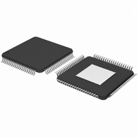
... NXP Semiconductors 14. Package outline HTQFP80: plastic thermal enhanced thin quad flat package; 80 leads; body mm; exposed die pad y exposed die pad pin 1 index DIMENSIONS (mm are the original dimensions) A UNIT max 0.15 1.05 0.27 mm 1.2 0.25 0.05 0.95 0.17 Note 1. Plastic or metal protrusions of 0.25 mm maximum per side are not included ...
Page 37
... NXP Semiconductors 15. Abbreviations Table 30. Acronym ACR AV CMOS CTS CTS/N DDC DE DTS DTV DVD DVI EAV EDID E-EDID FREF HBR HD HDCP HDMI HDTV HREF HSYNC KSV LSB LV-TTL MSB NTSC OTP PAL PCM PLL SAV SHA-1 S/PDIF TMDS VHREF VREF VSYNC YCbCr ...
Page 38
... NXP Semiconductors 16. Revision history Table 31. Revision history Document ID Release date TDA9984A_4 20090115 • Modifications: All document: changed Y-C • Section • Section • Figure • Table • Section HBR • Section • Section • Table • Table • Table and temperature max +85 C ...
Page 39
... Right to make changes — NXP Semiconductors reserves the right to make changes to information published in this document, including without limitation specifications and product descriptions, at any time and without notice ...
Page 40
... NXP Semiconductors 19. Contents 1 General description . . . . . . . . . . . . . . . . . . . . . . 1 2 Features . . . . . . . . . . . . . . . . . . . . . . . . . . . . . . . 1 3 Applications . . . . . . . . . . . . . . . . . . . . . . . . . . . . 2 4 Quick reference data . . . . . . . . . . . . . . . . . . . . . 3 5 Ordering information . . . . . . . . . . . . . . . . . . . . . 3 6 Block diagram . . . . . . . . . . . . . . . . . . . . . . . . . . 4 7 Pinning information . . . . . . . . . . . . . . . . . . . . . . 5 7.1 Pin description . . . . . . . . . . . . . . . . . . . . . . . . . 5 8 Functional description . . . . . . . . . . . . . . . . . . . 8 8.1 Video processing . . . . . . . . . . . . . . . . . . . . . . . 8 8.1.1 Internal assignment . . . . . . . . . . . . . . . . . . . . . 8 8.1.2 Input format mappings . . . . . . . . . . . . . . . . . . . 9 8.1.2.1 RGB external sync input (rising edge ...