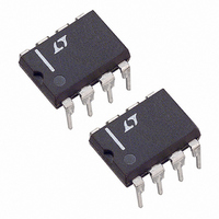
LTC1042CN8 Linear Technology, LTC1042CN8 Datasheet - Page 5

LTC1042CN8
Manufacturer Part Number
LTC1042CN8
Description
IC CMOS COMPARATOR WINDOW 8DIP
Manufacturer
Linear Technology
Series
LTCMOS™r
Type
Windowr
Datasheet
1.LTC1042CN8.pdf
(8 pages)
Specifications of LTC1042CN8
Number Of Elements
1
Output Type
TTL
Voltage - Supply
2.8 V ~ 16 V
Mounting Type
Through Hole
Package / Case
8-DIP (0.300", 7.62mm)
Lead Free Status / RoHS Status
Contains lead / RoHS non-compliant
Available stocks
Company
Part Number
Manufacturer
Quantity
Price
Company:
Part Number:
LTC1042CN8
Manufacturer:
NEC
Quantity:
5 510
Part Number:
LTC1042CN8
Manufacturer:
LINEAR/凌特
Quantity:
20 000
APPLICATIO S I FOR ATIO
To synchronize the sampling of the LTC1042 to an external
frequency source, the OSC pin can be driven by a CMOS
gate. A CMOS gate is necessary because the input trip
points of the oscillator are close to the supply rails and TTL
does not have enough output swing. Externally driven,
there will be a delay from the rising edge of the OSC input
and the start of the sampling cycle of approximately 5µs.
Input Impedance
The input impedance of the LTC1042 does not look like a
classic linear comparator; CMOS switches and a precision
capacitor array form the dual differential input structure.
Input impedance characteristics can be determined from
the equivalent circuit shown in Figure 2. The input
capacitance will charge with a time constant of R
is critical, in determining errors caused by the input
charging current, that C
“active” time.
For R
For Rs less than or equal to 10kΩ, C
error is caused by the charging current.
For R
For source resistances greater than 10kΩ, C
charge, causing voltage errors. To minimize these errors
an input bypass capacitor, C
shared between C
magnitude of this error is ∆V = V
error can be made arbitrarily small by increasing C
The averaging effect of the bypass capacitor C
another error term. Each time the input switches cycle
between the plus and minus inputs, C
discharged. The average input current due to this is
S
S
≤ 10kΩ
> 10kΩ
IN
U
and C
IN
U
S
be fully charged during the
causing a voltage error. The
S
should be used. Charge is
IN
W
IN
x C
fully charges and no
IN
IN
V
/(C
R
IN
is charged and
S
IN
IN
Figure 2. Equivalent Input Circuit
cannot fully
+ C
U
C
S
S
S
S
• C
causes
). This
+
–
S
.
IN
. It
S1
S2
LTC1042 DIFFERENTIAL INPUT
l
Because the input current is directly proportional to the
differential input voltage, the LTC1042 can be said to have
an average input resistance of R
Since two comparator inputs are connected in parallel, R
is one half this value (see typical curve of R
Frequency). This finite input resistance causes an error
due to voltage divided between R
The input error caused by both of these effects is
V
EXAMPLE: Assume f
V
sampling frequency is reduced to 1Hz, the voltage error
from input impedance effects is reduced to 136µV.
Input Voltage Range
The input switches of the LTC1042 are capable of
switching either to the V
the input voltage range includes both supply rails. This is
a further benefit of the input sampling structure.
Error Specifications
The only measurable errors on the LTC1042 are the
deviations from “ideal” of the upper and lower window
limits [Figure 1(B)]. The critical parameters for a window
comparator are the width and center of the window. These
errors may be expressed in terms of V
The specified error limits (see Electrical Characteristics)
include error due to offset, power supply variation, gain,
time and temperature.
AVG
ERROR
IN
center error = [(V
width error = (V
= 1V. Then V
= V
V
–
IN
= V
(~33pF)
~
x C
C
IN
IN
[2C
IN
LTC1042 • AI02
ERROR
x f
IN
S
/(2C
U
, where f
U
S
– V
= 1V(66µV + 660µV) = 726µV. If the
= 10Hz, R
+ V
IN
+
supply or ground. Consequently,
L
+ C
) – 2 x (WIDTH/2)
L
)/2] – CENTER
S
S
) + R
is the sampling frequency.
IN
S
= V
S
= 1MΩ, C
S
and R
/(R
IN
/I
U
S
LTC1042
AVG
and V
+ R
IN
IN
.
= 1/(f
vs Sampling
IN
S
)].
L
= 1µF and
.
S
x C
1042fa
5
IN
IN
).


