LTC1042CN8 Linear Technology, LTC1042CN8 Datasheet
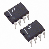
IC CMOS COMPARATOR WINDOW 8DIP

LTC1042CN8

Manufacturer Part Number
LTC1042CN8
Description
IC CMOS COMPARATOR WINDOW 8DIP
Manufacturer
Linear Technology
Series
LTCMOS™r
Type
Windowr
Datasheet

Specifications of LTC1042CN8

Number Of Elements
1
Output Type
TTL
Voltage - Supply
2.8 V ~ 16 V
Mounting Type
Through Hole
Package / Case
8-DIP (0.300", 7.62mm)
Lead Free Status / RoHS Status
Contains lead / RoHS non-compliant

Available stocks

Company
Part Number
Manufacturer
Quantity
Price
Part Number:
LTC1042CN8
Quantity:
5 510
Part Number:
LTC1042CN8
Manufacturer:
NEC
Quantity:
5 510
Part Number:
LTC1042CN8
Manufacturer:
LINEAR/凌特
Quantity:
20 000
FEATURES
APPLICATIO S
LTCMOS is a trademark of Linear Technology Corp.
TYPICAL APPLICATIO
T = YELLOW SPRINGS INSTRUMENT CO., INC. P/N 44007
ALL RESISTORS ±1% UNLESS OTHERWISE SPECIFIED
*OTHER TEMPERATURE BANDS MAY BE SELECTED BY CHOOSING APPROPRIATE VALUES FOR R1 AND R2
, LTC and LT are registered trademarks of Linear Technology Corporation.
Micropower 1.5µW (1 Sample/Second)
Wide Supply Range — 2.8V to 16V
High Accuracy
Wide Input Voltage Range
TTL Outputs with 5V Supply
Two Independent Ground-Referred Control Inputs
Small Size 8-Pin MiniDIP
Fault Detectors
Go/No-Go Testing
Microprocessor Power Supply Monitor
3V TO 16V
I
T
Center Error ±1mV Max
Width Error ±0.15% Max
V
+
to Ground
V
+
150k
R1*
7.5k
R2*
576Ω
Battery-Powered Remote Freezer Alarm
150k
U
T
1
2
3
4
LTC1042
U
8
7
6
5
10M ±5%
0.05µF
“HI” =
“HI” =
TEMPERATURE
BETWEEN
26°F AND 31°F
±1°F
TEMPERATURE
ABOVE 31°F
±1°F
LTC1042 • A01
DESCRIPTIO
The LTC
manufactured using Linear Technology’s enhanced
LTCMOS
voltage inputs, CENTER and WIDTH/2, define the middle
and width of the comparison window. Whenever the input
voltage, V
output is high. The ABOVE WINDOW output is high
whenever V
and CENTER, the ABOVE WINDOW output becomes
BELOW WINDOW and is high if V
Sampling techniques provide high impedance voltage
inputs that can common mode to both supply rails
(V
non-interaction. Also the device is effectively “chopper
stabilized,” giving it extremely high accuracy over
all conditions of temperature, power supply and input
voltage range.
Another benefit of the sampling techniques used to design
the LTC1042 is the extremely low power consumption.
When the device is strobed, it internally turns on the power
to the comparators, samples the inputs, stores the outputs
in CMOS latches and then turns off power to the compara-
tors. This all happens in about 80µs. Average power can be
made small, almost arbitrarily, by lowering the strobe rate.
The device can be self-strobed using an external RC
network or strobed externally by driving the OSC pin with
a CMOS gate.
+
and GND). An important feature of the inputs is their
®
1042 is a monolithic CMOS window comparator
IN
Window Comparator
silicon gate process. Two high impedance
IN
, is inside the window the WITHIN WINDOW
10000
1000
0.01
100
0.1
10
is above the window. By interchanging V
1
0.1
vs Sampling Frequency
V
+
U
Total Supply Current
SAMPLING FREQUENCY, f
= 6V
1
FOR THIS APPLICATION
f
S
I
T
≈ 1HZ
10
100
LTC1042 SUPPLY
CURRENT
IN
S
1000
(Hz)
is below the window.
LTC1042 • TA02
LTC1042
10000
1042fa
1
IN

Related parts for LTC1042CN8

LTC1042CN8 Summary of contents

Page 1

... TTL Outputs with 5V Supply Two Independent Ground-Referred Control Inputs Small Size 8-Pin MiniDIP U APPLICATIO S Fault Detectors Go/No-Go Testing Microprocessor Power Supply Monitor , LTC and LT are registered trademarks of Linear Technology Corporation. LTCMOS is a trademark of Linear Technology Corp. U TYPICAL APPLICATIO Battery-Powered Remote Freezer Alarm + V I ...

Page 2

... LTC1042C + = 4.75V –360µA OUT + = 4.75V –1.6mA OUT U W ORDER TOP VIEW + PART NUMBER OSC LTC1042CN8 ABOVE 3 6 WINDOW 4 5 WIDTH / 2 N8 PACKAGE 8-LEAD PDIP = 110 C, = 150 C/W JMAX JA J8 PACKAGE LTC1042MJ8 8-LEAD CERDIP MIN TYP MAX ±0.3 ± ±0.05 ± ...

Page 3

ELECTRICAL CHARACTERISTICS temperature range, otherwise specifications are at T SYMBOL PARAMETER TEST CONDITIONS R External Timing Resistor Resistor connected between V EXT and OSC Pin f Sampling Frequency Note 1: Absolute Maximum Ratings are those values beyond ...

Page 4

LTC1042 U U APPLICATIO S I FOR ATIO The LTC1042 uses sampled data techniques to achieve its unique characteristics. It consists of two comparators, each of which has two differential inputs (Figure 1). When the sum of the voltages on ...

Page 5

U U APPLICATIO S I FOR ATIO To synchronize the sampling of the LTC1042 to an external frequency source, the OSC pin can be driven by a CMOS gate. A CMOS gate is necessary because the input trip points of ...

Page 6

LTC1042 U U APPLICATIO S I FOR ATIO 25k LT1004-2.5 ALL RESISTORS ± 5% UNLESS OTHERWISE NOTED SUPPLY TOLERANCE EQUALS R2 IN kΩ. I.E., 10k = ±10% * COLD JUNCTION COMPENSATOR 36k 5% R4 † 1690 ...

Page 7

... BATTERY 10k LT1004-1.2 Information furnished by Linear Technology Corporation is believed to be accurate and reliable. However, no responsibility is assumed for its use. Linear Technology Corporation makes no represen- tation that the interconnection of its circuits as described herein will not infringe on existing patent rights the generator voltage output is between 13.8V and 15 ...

Page 8

... RAD TYP .125 3.175 MIN .130 ± .005 (3.302 ± 0.127) .120 .020 (3.048) MIN (0.508) MIN .018 ± .003 (0.457 ± 0.076) N8 1002 LW/TP 1202 1K REV A • PRINTED IN USA  LINEAR TECHNOLOGY CORPORATION 1988 .220 – .310 J8 0801 1042fa ...

Related keywords