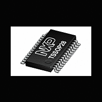
P89LPC930_931 NXP Semiconductors, P89LPC930_931 Datasheet - Page 25

P89LPC930_931
Manufacturer Part Number
P89LPC930_931
Description
The P89LPC930/931 are single-chip microcontrollers designed for applicationsdemanding high-integration, low cost solutions over a wide range of performancerequirements
Manufacturer
NXP Semiconductors
Datasheet
1.P89LPC930_931.pdf
(55 pages)
Philips Semiconductors
9397 750 14472
Product data
8.13.1 Idle mode
8.13.2 Power-down mode
8.13.3 Total Power-down mode
8.14 Reset
Idle mode leaves peripherals running in order to allow them to activate the processor
when an interrupt is generated. Any enabled interrupt source or reset may terminate
Idle mode.
The Power-down mode stops the oscillator in order to minimize power consumption.
The P89LPC930/931 exits Power-down mode via any reset, or certain interrupts. In
Power-down mode, the power supply voltage may be reduced to the RAM keep-alive
voltage V
was entered. SFR contents are not guaranteed after V
therefore it is highly recommended to wake up the processor via reset in this case.
V
exited.
Some chip functions continue to operate and draw power during Power-down mode,
increasing the total power used during Power-down. These include: Brownout detect,
Watchdog Timer, Comparators (note that Comparators can be powered-down
separately), and Real-Time Clock (RTC)/System Timer. The internal RC oscillator is
disabled unless both the RC oscillator has been selected as the system clock and the
RTC is enabled.
This is the same as Power-down mode except that the brownout detection circuitry
and the voltage comparators are also disabled to conserve additional power. The
internal RC oscillator is disabled unless both the RC oscillator has been selected as
the system clock and the RTC is enabled. If the internal RC oscillator is used to clock
the RTC during Power-down, there will be high power consumption. Please use an
external low frequency clock to achieve low power with the Real-Time Clock running
during Power-down.
The P1.5/RST pin can function as either an active-LOW reset input or as a digital
input, P1.5. The RPE (Reset Pin Enable) bit in UCFG1, when set to ‘1’, enables the
external reset input function on P1.5. When cleared, P1.5 may be used as an input
pin.
Remark: During a power-up sequence, the RPE selection is overridden and this pin
will always function as a reset input. An external circuit connected to this pin
should not hold this pin LOW during a power-on sequence as this will keep the
device in reset. After power-up this input will function either as an external reset
input or as a digital input as defined by the RPE bit. Only a power-up reset will
temporarily override the selection defined by RPE bit. Other sources of reset will not
override the RPE bit.
Remark: During a power cycle, V
characteristics” on page
reset.
Reset can be triggered from the following sources:
DD
must be raised to within the operating range before the Power-down mode is
RAM
. This retains the RAM contents at the point where Power-down mode
Rev. 05 — 15 December 2004
42) before power is reapplied, in order to ensure a power-on
8-bit microcontrollers with two-clock 80C51 core
DD
must fall below V
P89LPC930/931
POR
© Koninklijke Philips Electronics N.V. 2004. All rights reserved.
DD
has been lowered to V
(see
Table 7 “DC electrical
25 of 55
RAM
,


