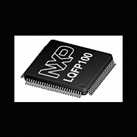
LPC2157_2158 NXP Semiconductors, LPC2157_2158 Datasheet - Page 14

LPC2157_2158
Manufacturer Part Number
LPC2157_2158
Description
The LPC2157/2158 is a multi-chip module consisting of a LPC2138/2148 single-chipmicrocontroller combined with a PCF8576D Universal LCD driver in a low-cost 100-pinpackage
Manufacturer
NXP Semiconductors
Datasheet
1.LPC2157_2158.pdf
(45 pages)
NXP Semiconductors
Table 3.
[1]
[2]
[3]
[4]
[5]
[6]
[7]
[8]
[9]
LPC2157_2158_2
Product data sheet
Symbol
V
V
V
V
VREF
VBAT
SDA_LCD
SCL_LCD
SYNC
CLK
BP0 to BP3
S0 to S31
DD
DDA
DD(LCD)
LCD
5 V tolerant pad providing digital I/O functions with TTL levels and hysteresis and 10 ns slew rate control.
5 V tolerant pad providing digital I/O functions with TTL levels and hysteresis and 10 ns slew rate control. If configured for an input
function, this pad utilizes built-in glitch filter that blocks pulses shorter than 3 ns.
Open-drain 5 V tolerant digital I/O I
functionality.
5 V tolerant pad providing digital I/O (with TTL levels and hysteresis and 10 ns slew rate control) and analog input function. If configured
for an input function, this pad utilizes built-in glitch filter that blocks pulses shorter than 3 ns. When configured as an ADC input, digital
section of the pad is disabled.
5 V tolerant pad providing digital I/O (with TTL levels and hysteresis and 10 ns slew rate control) and analog output function. When
configured as the DAC output, digital section of the pad is disabled.
5 V tolerant pad with built-in pull-up resistor providing digital I/O functions with TTL levels and hysteresis and 10 ns slew rate control.
The pull-up resistor’s value typically ranges from 60 k to 300 k .
Pad is designed in accordance with the Universal Serial Bus (USB) specification, revision 2.0 (Full-speed and Low-speed mode only).
5 V tolerant pad providing digital input (with TTL levels and hysteresis) function only.
Pad provides special analog functionality.
Pin description LPC2158
Pin
11, 27, 33 I
96
38
41
89
31
34
35
36
37
42 to 45
46 to 77
Type
I
I
I
I
I
I/O
I
I/O
I/O
O
O
2
C-bus 400 kHz specification compatible pad. It requires external pull-up to provide an output
…continued
Description
3.3 V power supply: This is the power supply voltage for the core and I/O
ports.
Analog 3.3 V power supply: This should be nominally the same voltage as
V
used to power the on-chip ADC(s) and DAC.
1.8 V to 5.5 V power supply: Power supply voltage for the PCF8576D.
LCD power supply: LCD voltage.
ADC reference voltage: This should be nominally less than or equal to the
V
pin is used as a reference for ADC(s) and DAC.
RTC power supply voltage: 3.3 V on this pin supplies the power to the RTC.
SDA LCD — I
SCL LCD — I
SYNC — cascade synchronization input/output
CLK — external clock input/output
BP0 to BP3: LCD backplane outputs.
S0 to S31: LCD segment outputs.
DD
DD
Rev. 02 — 9 February 2009
but should be isolated to minimize noise and error. This voltage is only
voltage but should be isolated to minimize noise and error. Level on this
2
2
C-bus clock signal for the LCD controller.
C-bus data signal for the LCD controller.
Single-chip 16-bit/32-bit microcontrollers
LPC2157/2158
© NXP B.V. 2009. All rights reserved.
14 of 45


