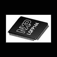
LPC1788FBD144 NXP Semiconductors, LPC1788FBD144 Datasheet - Page 35

LPC1788FBD144
Manufacturer Part Number
LPC1788FBD144
Description
The LPC1788 is a Cortex-M3 microcontroller for embedded applications featuring a high level of integration and low power consumption at frequencies of 120 MHz
Manufacturer
NXP Semiconductors
Datasheet
1.LPC1774FBD144.pdf
(120 pages)
Available stocks
Company
Part Number
Manufacturer
Quantity
Price
Company:
Part Number:
LPC1788FBD144
Manufacturer:
ELPIDA
Quantity:
1 043
Part Number:
LPC1788FBD144
Manufacturer:
NXP/恩智浦
Quantity:
20 000
NXP Semiconductors
Table 3.
Not all functions are available on all parts. See
pins).
[1]
[2]
[3]
[4]
[5]
[6]
[7]
[8]
[9]
[10] 5 V tolerant pad with 5 ns glitch filter providing digital I/O functions with TTL levels and hysteresis.
[11] <tbd>
[12] 5 V tolerant pad with 20 ns glitch filter providing digital I/O function with TTL levels and hysteresis.
[13] <tbd>
[14] Pad provides special analog functionality.
[15] If the RTC is not used, these pins can be left floating.
[16] When the main oscillator is not used, connect XTAL1 and XTAL2 as follows: XTAL1 can be left floating or can be grounded (grounding
LPC178X_7X
Objective data sheet
Symbol
V
V
V
XTAL1
XTAL2
SS
SSREG
SSA
PU = internal pull-up enabled (for V
pins, if not used, should be tied to ground or power to minimize power consumption.
I = Input; O = Output; G = Ground; S = Supply.
5 V tolerant pad providing digital I/O functions with TTL levels and hysteresis.
<tbd>
5 V tolerant pad providing digital I/O functions with TTL levels and hysteresis and analog input. When configured as a ADC input, digital
section of the pad is disabled.
<tbd>
5 V tolerant pad providing digital I/O with TTL levels and hysteresis and analog output function. When configured as the DAC output,
digital section of the pad is disabled.
Open-drain 5 V tolerant digital I/O pad, compatible with I
functionality. When power is switched off, this pin connected to the I
configuration applies to all functions on this pin.
Not 5 V tolerant. Pad provides digital I/O and USB functions. It is designed in accordance with the USB specification, revision 2.0
(Full-speed and Low-speed mode only).
is preferred to reduce susceptibility to noise). XTAL2 should be left floating.
Pin description
33,
63,
77,
93,
114,
133,
148,
169,
189,
200
32,
84,
172
22
44
46
L3,
T5,
R9,
P12,
N16,
H14,
E15,
A12,
B6,
A2
D12,
K4,
P10
J2
M4
N4
…continued
H4,
P4,
L9,
L13,
G13,
D13,
C11,
B4
H3,
L8,
A10
F3
L2
K4
44,
65,
79,
103,
117,
139
22,
59,
119
15
31
33
DD(REG)(3V3)
[14]
[16]
[14]
[16]
All information provided in this document is subject to legal disclaimers.
= 3.3 V, pulled up to 3.3 V); IA = inactive, no pull-up/down enabled; F = floating; floating
Table 2
Rev. 3 — 27 December 2011
G
G
G
I
O
2
(Ethernet, USB, LCD, QEI, SD/MMC, DAC pins) and
C-bus 400 kHz specification. It requires an external pull-up to provide output
Description
Ground: 0 V reference for digital IO pins.
Ground: 0 V reference for internal logic.
Analog ground: 0 V power supply and reference for the ADC
and DAC. This should be the same voltage as V
be isolated to minimize noise and error.
Input to the oscillator circuit and internal clock generator circuits.
Output from the oscillator amplifier.
2
C-bus is floating and does not disturb the I
32-bit ARM Cortex-M3 microcontroller
LPC178x/7x
2
C lines. Open-drain
© NXP B.V. 2011. All rights reserved.
SS
Table 7
, but should
35 of 120
(EMC


