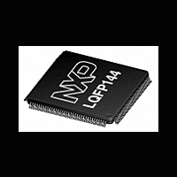
LPC1788FBD144 NXP Semiconductors, LPC1788FBD144 Datasheet - Page 34

LPC1788FBD144
Manufacturer Part Number
LPC1788FBD144
Description
The LPC1788 is a Cortex-M3 microcontroller for embedded applications featuring a high level of integration and low power consumption at frequencies of 120 MHz
Manufacturer
NXP Semiconductors
Datasheet
1.LPC1774FBD144.pdf
(120 pages)
Available stocks
Company
Part Number
Manufacturer
Quantity
Price
Company:
Part Number:
LPC1788FBD144
Manufacturer:
ELPIDA
Quantity:
1 043
Part Number:
LPC1788FBD144
Manufacturer:
NXP/恩智浦
Quantity:
20 000
NXP Semiconductors
Table 3.
Not all functions are available on all parts. See
pins).
LPC178X_7X
Objective data sheet
Symbol
JTAG_TMS
(SWDIO)
JTAG_TRST
JTAG_TCK
(SWDCLK)
RESET
RSTOUT
RTC_ALARM
RTCX1
RTCX2
USB_D2
VBAT
V
V
V
VREFP
DD(REG)(3V3)
DDA
DD(3V3)
Pin description
6
8
10
35
29
37
34
36
52
38
26,
86,
174
20
15,
60,
71,
89,
112,
125,
146,
165,
181,
198
24
E3
D1
E2
M2
K3
N1
K2
L2
U1
M3
H4,
P11,
D11
G4
G3,
P6,
P8,
U13,
P17,
K16,
C17,
B13,
C9,
D7
K1
…continued
H5
K1
F2
C2
D4
D2
J1
H2
J2
J3
N2
G1,
N9,
E9
E2,
L4,
K8,
L11,
J14,
E12,
E10,
C5
G2
4
5
7
24
20
26
23
25
37
27
18,
60,
121
14
41,
62,
77,
102,
114,
138
17
[3]
[3]
[3]
[12]
[3]
[13]
[14]
[15]
[14]
[15]
[9]
All information provided in this document is subject to legal disclaimers.
<tb
d>
Table 2
Rev. 3 — 27 December 2011
I
I
I
I
O
O
I
O
I/O
I
S
S
S
S
(Ethernet, USB, LCD, QEI, SD/MMC, DAC pins) and
Description
Test Mode Select for JTAG interface. Also used as Serial wire
debug data input/output.
Test Reset for JTAG interface.
Test Clock for JTAG interface. This clock must be slower than
1 /6 of the CPU clock (CCLK) for the JTAG interface to operate.
Also used as serial wire clock.
External reset input. A LOW on this pin resets the device,
causing I/O ports and peripherals to take on their default states,
and processor execution to begin at address 0. This pin includes
a 20 ns input glitch filter.
Reset status output. A LOW output on this pin indicates that the
device is in the reset state for any reason. This reflects the
RESET input pin and all internal reset sources.
RTC controlled output. This is a 1.8 V pin. It goes HIGH when a
RTC alarm is generated.
Input to the RTC 32 kHz ultra-low power oscillator circuit.
Output from the RTC 32 kHz ultra-low power oscillator circuit.
USB port 2 bidirectional D line.
RTC power supply: 3.3 V on this pin supplies power to the RTC.
3.3 V regulator supply voltage: This is the power supply for the
on-chip voltage regulator that supplies internal logic.
Analog 3.3 V pad supply voltage: This can be connected to the
same supply as V
noise and error. This voltage is used to power the ADC and
DAC. Tie this pin to 3.3 V if the ADC and DAC are not used.
3.3 V supply voltage: This is the power supply voltage for I/O
other than pins in the VBAT domain.
ADC positive reference voltage: This should be the same
voltage as V
error. The voltage level on this pin is used as a reference for
ADC and DAC. Tie this pin to 3.3 V if the ADC and DAC are not
used.
DDA
, but should be isolated to minimize noise and
DD(3V3)
32-bit ARM Cortex-M3 microcontroller
but should be isolated to minimize
LPC178x/7x
© NXP B.V. 2011. All rights reserved.
Table 7
34 of 120
(EMC


