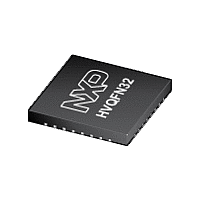
LPC1114FHN33 NXP Semiconductors, LPC1114FHN33 Datasheet - Page 48

LPC1114FHN33
Manufacturer Part Number
LPC1114FHN33
Description
The LPC1114FHN33 is an ARM Cortex-M0 microcontroller and it can operate up to 50 MHz
Manufacturer
NXP Semiconductors
Datasheet
1.LPC1110FD20.pdf
(103 pages)
Available stocks
Company
Part Number
Manufacturer
Quantity
Price
Company:
Part Number:
LPC1114FHN33
Manufacturer:
NXP
Quantity:
2 000
Part Number:
LPC1114FHN33
Manufacturer:
NXP/恩智浦
Quantity:
20 000
Company:
Part Number:
LPC1114FHN33/201
Manufacturer:
NXP
Quantity:
306
Part Number:
LPC1114FHN33/201
Manufacturer:
NXP/恩智浦
Quantity:
20 000
Company:
Part Number:
LPC1114FHN33/202
Manufacturer:
NXP
Quantity:
201
Part Number:
LPC1114FHN33/202
Manufacturer:
NXP/恩智浦
Quantity:
20 000
Company:
Part Number:
LPC1114FHN33/301
Manufacturer:
NXP
Quantity:
2 000
Company:
Part Number:
LPC1114FHN33/301
Manufacturer:
EVERLIGHT
Quantity:
30 030
Part Number:
LPC1114FHN33/301
Manufacturer:
NXP/恩智浦
Quantity:
20 000
Part Number:
LPC1114FHN33/302
Manufacturer:
NXP/恩智浦
Quantity:
20 000
NXP Semiconductors
LPC111X
Product data sheet
7.16.1.3 Watchdog oscillator
7.16.5.1 Power profiles (LPC1100L and LPC1100XL series only)
7.16.2 System PLL
7.16.3 Clock output
7.16.4 Wake-up process
7.16.5 Power control
The watchdog oscillator can be used as a clock source that directly drives the CPU, the
watchdog timer, or the CLKOUT pin. The watchdog oscillator nominal frequency is
programmable between 7.8 kHz and 1.7 MHz. The frequency spread over processing and
temperature is 40 %.
The PLL accepts an input clock frequency in the range of 10 MHz to 25 MHz. The input
frequency is multiplied up to a high frequency with a Current Controlled Oscillator (CCO).
The multiplier can be an integer value from 1 to 32. The CCO operates in the range of
156 MHz to 320 MHz, so there is an additional divider in the loop to keep the CCO within
its frequency range while the PLL is providing the desired output frequency. The PLL
output frequency must be lower than 100 MHz. The output divider may be set to divide by
2, 4, 8, or 16 to produce the output clock. Since the minimum output divider value is 2, it is
insured that the PLL output has a 50 % duty cycle. The PLL is turned off and bypassed
following a chip reset and may be enabled by software. The program must configure and
activate the PLL, wait for the PLL to lock, and then connect to the PLL as a clock source.
The PLL settling time is 100 s.
The LPC1110/11/12/13/14/15 features a clock output function that routes the IRC
oscillator, the system oscillator, the watchdog oscillator, or the main clock to an output pin.
The LPC1110/11/12/13/14/15 begin operation at power-up and when awakened from
Deep power-down mode by using the 12 MHz IRC oscillator as the clock source. This
allows chip operation to resume quickly. If the system oscillator or the PLL is needed by
the application, software will need to enable these features and wait for them to stabilize
before they are used as a clock source.
The LPC1110/11/12/13/14/15 support a variety of power control features. There are three
special modes of processor power reduction: Sleep mode, Deep-sleep mode, and Deep
power-down mode. The CPU clock rate may also be controlled as needed by changing
clock sources, reconfiguring PLL values, and/or altering the CPU clock divider value. This
allows a trade-off of power versus processing speed based on application requirements.
In addition, a register is provided for shutting down the clocks to individual on-chip
peripherals, allowing fine tuning of power consumption by eliminating all dynamic power
use in any peripherals that are not required for the application. Selected peripherals have
their own clock divider which provides even better power control.
The power consumption in Active and Sleep modes can be optimized for the application
through simple calls to the power profile. The power configuration routine configures the
LPC1110/11/12/13/14/15 for one of the following power modes:
•
•
Default mode corresponding to power configuration after reset.
CPU performance mode corresponding to optimized processing capability.
All information provided in this document is subject to legal disclaimers.
Rev. 7 — 1 March 2012
LPC1110/11/12/13/14/15
32-bit ARM Cortex-M0 microcontroller
© NXP B.V. 2012. All rights reserved.
48 of 103


