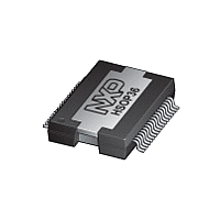
TDF8599B NXP Semiconductors, TDF8599B Datasheet - Page 29

TDF8599B
Manufacturer Part Number
TDF8599B
Description
The TDF8599B is a dual Bridge-Tied Load (BTL) car audio amplifier comprising anNDMOST-NDMOST output stage based on SOI BCDMOS technology
Manufacturer
NXP Semiconductors
Datasheet
1.TDF8599B.pdf
(54 pages)
Available stocks
Company
Part Number
Manufacturer
Quantity
Price
Part Number:
TDF8599BTH
Manufacturer:
NXP/恩智浦
Quantity:
20 000
Company:
Part Number:
TDF8599BTH/N1,518
Manufacturer:
NXP
Quantity:
210
NXP Semiconductors
Table 19.
V
TDF8599B_1
Product data sheet
Symbol
Diagnostic output
THD
V
V
I
Audio inputs; pins IN1N, IN1P, IN2N and IN2P
V
SVRR voltage and ACGND input bias voltage in Mute and Operating modes
V
Amplifier outputs; pins OUT1N, OUT1P, OUT2N and OUT2P
V
Stabilizer output; pins VSTAB1 and VSTAB2
V
Voltage protections
V
Current protection
I
Temperature protection
T
T
T
T
DC load detection levels: I
Z
Z
AC load detection levels: I
I
L
O(ocp)
th(o)det(load)AC
P
prot
act(th_fold)
j(AV)(warn1)
j(AV)(warn2)
th(load)
th(open)
th(offset)
OL
i
ref
O(offset)
o
(prot)
= V
clip
DDA
= 14.4 V; f
Static characteristics
Parameter
total harmonic distortion clip
detection level
threshold voltage for offset
detection
LOW-level output voltage
leakage current
input voltage
reference voltage
output offset voltage
output voltage
protection voltage
overcurrent protection output
current
protection temperature
thermal foldback activation
temperature
average junction temperature
for pre-warning 1
average junction temperature
for pre-warning 2
load detection threshold
impedance
open load detection threshold
impedance
AC load detection output
threshold current
osc
= 320 kHz; 40 C < T
2
2
C-bus mode only
C-bus mode only
…continued
amb
[7]
< +85 C; unless otherwise specified.
Rev. 01 — 29 July 2009
Conditions
DIAG or CLIP pins activated;
I
DIAG and CLIP pins; diagnostic
not activated
input ACGND pin
half supply reference SVRR pin
BTL; Mute mode
BTL; Operating mode
stabilizer output in Mute mode and
Operating mode
undervoltage; amplifier is muted
overvoltage; load dump protection
is activated
V
current limiting concept
gain = 1 dB
IB2[D3] = 0; non-I
IB2[D3] = 1
for normal speaker load;
DB1[D4] = 0; DB2[D4] = 0
DB1[D4] = 1; DB2[D4] = 1
o
P
= 1 mA
that a POR occurs at
I
2
C-bus controlled dual channel class-D power amplifier
2
C-bus mode
[2][3]
[4][6]
Min
-
1
-
-
-
2
6.9
-
-
8
6.8
26.2
3
8
155
140
-
-
-
350
250
TDF8599B
Typ
0.2
2
-
-
2.45
2.45
7.2
-
-
10
7.2
27
3.7
9.5
-
-
140
120
-
-
500
© NXP B.V. 2009. All rights reserved.
Max
-
3
0.3
50
-
3
7.5
25
70
12
8
-
4.6
11
160
150
150
130
25
-
700
29 of 54
Unit
%
V
V
V
V
V
mV
mV
V
V
V
V
A
mA
C
C
C
C
A


