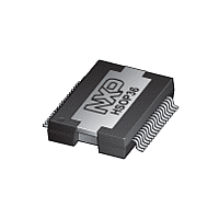
TDF8599A NXP Semiconductors, TDF8599A Datasheet - Page 17

TDF8599A
Manufacturer Part Number
TDF8599A
Description
The TDF8599A is a dual Bridge-Tied Load (BTL) car audio amplifier comprising anNDMOST-NDMOST output stage based on SOI BCDMOS technology
Manufacturer
NXP Semiconductors
Datasheet
1.TDF8599A.pdf
(54 pages)
Available stocks
Company
Part Number
Manufacturer
Quantity
Price
Part Number:
TDF8599ATD
Manufacturer:
NXP/恩智浦
Quantity:
20 000
Part Number:
TDF8599ATH
Manufacturer:
NXP/恩智浦
Quantity:
20 000
NXP Semiconductors
TDF8599A_2
Product data sheet
8.5.6 Supply voltages
8.5.7 Overview of protection circuits and amplifier states
8.6.1 Diagnostic table
8.6 Diagnostic output
In non-I
information on pin DIAG and shuts down both channels.
Connecting a capacitor between pins DCP and AGND enables DC offset protection.
Connecting pin DCP to pin AGND disables DCP in both I
UnderVoltage Protection (UVP) is activated when the supply voltage drops below the UVP
threshold. UVP triggers the UVP circuit causing the system to first mute and then stop
switching. When the supply voltage rises above the threshold level, the system restarts.
OverVoltage Protection (OVP) is activated when the supply voltage exceeds the OVP
threshold. The OVP (or load dump) circuit is activated and the power stages are
shutdown.
An overview of all protection circuits and the amplifier states is given in
Table 10.
[1]
[2]
[3]
[4]
[5]
[6]
The diagnostic information for I
The instruction bitmap and data bytes are described in
Pins DIAG and CLIP have an open-drain output which must have an external pull-up
resistor connected to an external voltage. Pins CLIP and DIAG can show both fixed and
I
Protection circuit name
TFP
OTP
OCP
WP
DCP
UVP
OVP
2
C-bus selectable information.
When fault is removed.
Amplifier gain depends on the junction temperature and size of the heat sink.
TFP influences restart timing depending on heat sink size.
Shorted load causes a restart of the channel every 50 ms.
Latched protection is reset by toggling pin EN or by disabling DCP in I
In I
I
2
C-bus command.
2
C-bus mode deep supply voltage drops will cause a Power-On Reset (POR). The restart requires an
2
C-bus mode, when an offset is detected, DCP always gives diagnostic
Overview of TDF8599A protection circuits and amplifier states
Rev. 02 — 30 June 2009
I
2
2
C-bus controlled dual channel class-D power amplifier
C-bus mode and non-I
Amplifier state
Complete
shutdown
N
Y
N
N
Y
Y
Y
[2]
2
C-bus mode is shown in
Table 14
Channel
shutdown
N
N
Y
Y
N
N
N
2
[2]
C-bus and non-I
2
C-bus mode.
and
TDF8599A
Table
© NXP B.V. 2009. All rights reserved.
Table
Restart
Y
Y
Y
Y
N
Y
Y
2
[3]
[3]
[4]
[6]
[5]
15.
C-bus mode.
10.
Table
[1]
17 of 54
11.


