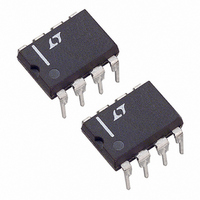
LT1011ACN8#PBF Linear Technology, LT1011ACN8#PBF Datasheet - Page 9

LT1011ACN8#PBF
Manufacturer Part Number
LT1011ACN8#PBF
Description
IC VOLTAGE COMPARATOR 5V 8-DIP
Manufacturer
Linear Technology
Type
General Purposer
Datasheet
1.LT1011CN8PBF.pdf
(16 pages)
Specifications of LT1011ACN8#PBF
Number Of Elements
1
Output Type
Open Collector
Voltage - Supply
3 V ~ 36 V, ±1.5 V ~ 18 V
Mounting Type
Through Hole
Package / Case
8-DIP (0.300", 7.62mm)
Comparator Type
General Purpose
No. Of Comparators
1
Response Time
150ns
Ic Output Type
Open Collector
Supply Current
3.2mA
Supply Voltage Range
3V To ± 18V
Amplifier Case Style
DIP
Rohs Compliant
Yes
Number Of Elements
1
Technology
Bipolar
Input Offset Voltage
750uV
Input Bias Current (typ)
25nA
Single Supply Voltage (typ)
9/12/15/18/24/28V
Dual Supply Voltage (typ)
±3/±5/±9/±12V
Supply Current (max)
4@±15VmA
Power Supply Requirement
Single/Dual
Common Mode Rejection Ratio
115dB
Voltage Gain In Db
113.98dB
Single Supply Voltage (min)
5V
Single Supply Voltage (max)
30V
Dual Supply Voltage (min)
±2.5V
Dual Supply Voltage (max)
±15V
Operating Temp Range
0C to 70C
Operating Temperature Classification
Commercial
Mounting
Through Hole
Pin Count
8
Package Type
PDIP N
Lead Free Status / RoHS Status
Lead free / RoHS Compliant
Available stocks
Company
Part Number
Manufacturer
Quantity
Price
APPLICATIONS INFORMATION
In the “off” state, I
turn off. The collector of Q2 can be now held at any voltage
above V
above the positive supply level. Maximum voltage above
V
emitter can be held at any voltage between V
long as it is negative with respect to the collector.
In the “on” state, I
Diodes D1 and D2 prevent deep saturation of Q2 to improve
speed and also limit the drive current of Q1. The R1/R2
divider sets the saturation voltage of Q2 and provides turn-
off drive. Either the collector or emitter pin can be held at
a voltage between V
pin to drive the load. In typical applications, the emitter is
connected to V
tied to V
When the emitter is used as the output, the collector is
typically tied to V
or V
respect to the collector output so that the “+” and “–”
input designations must be reversed. When the collector
TYPICAL APPLICATIONS
–
is 50V for the LT1011M and 40V for the LT1011C/I. The
–
. Note that the emitter output is phase reversed with
Offset Balancing
2
3
–
+
+
–
without conducting current, including voltages
or a separate positive supply.
5
LT1011
20k
R1
R2
3k
–
6
or ground and the collector drives a load
8
+
1
1
and the load is connected to ground
7
is connected, turning on Q1 and Q2.
+
1011 TA03
is switched off and both Q1 and Q2
and V
V
+
–
. This allows the remaining
V
++
+
Driving Load Referenced
CAN BE GREATER OR LESS THAN V
and V
3
2
to Positive Supply
–
+
LT1011
–
V
V
as
+
8
4
GROUND
OR
V
1
7
is tied to V
about 2V below V
Input Signal Range
The common mode input voltage range of the LT1011 is
about 300mV above the negative supply and 1.5V below the
positive supply, independent of the actual supply voltages
(see curve in the Typical Performance Characteristics). This
is the voltage range over which the output will respond
correctly when the common mode voltage is applied to
one input and a higher or lower signal is applied to the
remaining input. If one input is inside the common mode
range and one is outside, the output will be correct. If the
inputs are outside the common mode range in opposite
directions, the output will still be correct. If both inputs are
outside the common mode range in the same direction,
the output will not respond to the differential input; for
temperatures of 25°C and above, the output will remain
unconditionally high (collector output), for temperatures
below 25°C, the output becomes undefi ned.
V
1011 TA05
++
R
LOAD
+
+
, the voltage at the emitter in the “on” state is
+
(see curves).
LT1011/LT1011A
INPUTS*
Driving Load Referenced
*INPUT POLARITY IS REVERSED
WHEN USING PIN 1 AS OUTPUT
to Negative Supply
2
3
–
+
LT1011
4
V
+
8
V
1
R
7
LOAD
1011 TA06
V
1011afc
9


