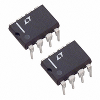
LT1011ACN8#PBF Linear Technology, LT1011ACN8#PBF Datasheet - Page 6

LT1011ACN8#PBF
Manufacturer Part Number
LT1011ACN8#PBF
Description
IC VOLTAGE COMPARATOR 5V 8-DIP
Manufacturer
Linear Technology
Type
General Purposer
Datasheet
1.LT1011CN8PBF.pdf
(16 pages)
Specifications of LT1011ACN8#PBF
Number Of Elements
1
Output Type
Open Collector
Voltage - Supply
3 V ~ 36 V, ±1.5 V ~ 18 V
Mounting Type
Through Hole
Package / Case
8-DIP (0.300", 7.62mm)
Comparator Type
General Purpose
No. Of Comparators
1
Response Time
150ns
Ic Output Type
Open Collector
Supply Current
3.2mA
Supply Voltage Range
3V To ± 18V
Amplifier Case Style
DIP
Rohs Compliant
Yes
Number Of Elements
1
Technology
Bipolar
Input Offset Voltage
750uV
Input Bias Current (typ)
25nA
Single Supply Voltage (typ)
9/12/15/18/24/28V
Dual Supply Voltage (typ)
±3/±5/±9/±12V
Supply Current (max)
4@±15VmA
Power Supply Requirement
Single/Dual
Common Mode Rejection Ratio
115dB
Voltage Gain In Db
113.98dB
Single Supply Voltage (min)
5V
Single Supply Voltage (max)
30V
Dual Supply Voltage (min)
±2.5V
Dual Supply Voltage (max)
±15V
Operating Temp Range
0C to 70C
Operating Temperature Classification
Commercial
Mounting
Through Hole
Pin Count
8
Package Type
PDIP N
Lead Free Status / RoHS Status
Lead free / RoHS Compliant
Available stocks
Company
Part Number
Manufacturer
Quantity
Price
LT1011/LT1011A
TYPICAL PERFORMANCE CHARACTERISTICS
APPLICATIONS INFORMATION
Preventing Oscillation Problems
Oscillation problems in comparators are nearly always
caused by stray capacitance between the output and
inputs or between the output and other sensitive pins
on the comparator. This is especially true with high
gain bandwidth comparators like the LT1011, which are
designed for fast switching with millivolt input signals.
The gain bandwidth product of the LT1011 is over 10GHz.
Oscillation problems tend to occur at frequencies around
5MHz, where the LT1011 has a gain of ≈2000. This implies
that attenuation of output signals must be at least 2000:1 at
5MHz as measured at the inputs. If the source impedance
is 1kΩ, the effective stray capacitance between output and
input must have a reactance of more than (2000)(1kΩ) =
2MΩ, or less than 0.02pF . The actual interlead capacitance
between input and output pins on the LT1011 is less than
0.002pF when cut to printed circuit mount length. Additional
stray capacitance due to printed circuit traces must be
minimized by routing the output trace directly away from
input lines and, if possible, running ground traces next
to input traces to provide shielding. Additional steps to
ensure oscillation-free operation are:
1. Bypass the STROBE/BALANCE pins with a 0.01μF
6
capacitor connected from Pin 5 to Pin 6. This elimi-
nates stray capacitive feedback from the output to
–0.5
–1.0
–1.5
–2.0
–2.5
2.5
2.0
1.5
1.0
0.5
0
V
Input Offset Voltage
vs Common Mode Voltage
–
T
J
0.1 0.2 0.3 0.4 0.5 0.6 0.7
= 25°C
V
SINGLE SUPPLY)
–
COMMON MODE VOLTAGE (V)
(OR GND WITH
LIMIT = V
COMMON MODE
+
– (1.5V)
UPPER
1011 G19
V
+
2. Bypass the negative supply (Pin 4) with a 0.1μF
3. Bypass any slow moving or DC input with a capaci-
4. Keep resistive source impedance as low as possible.
5. Use hysteresis. This consists of shifting the input
the BALANCE pins, which are nearly as sensitive as
the inputs.
ceramic capacitor close to the comparator. 0.1μF can
also be used for the positive supply (Pin 8) if the
pull-up load is tied to a separate supply. When the
pull-up load is tied directly to Pin 8, use a 2μF solid
tantalum bypass capacitor.
tor (≥0.01μF) close to the comparator to reduce high
frequency source impedance.
If a resistor is added in series with one input to bal-
ance source impedances for DC accuracy, bypass
it with a capacitor. The low input bias current of the
LT1011 usually eliminates any need for source resis-
tance balancing. A 5kΩ imbalance, for instance, will
create only 0.25mV DC offset.
offset voltage of the comparator when the output
changes state. Hysteresis forces the comparator to
move quickly through its linear region, eliminating
oscillations by “overdriving” the comparator under all
input conditions. Hysteresis may be either AC or DC.
AC techniques do not shift the apparent offset voltage
–150mV
–100mV
–50mV
0.8
0.6
0.4
0.2
0
0
–50 –25
Offset Pin Characteristics
CHANGE IN V
VOLTAGE ON PINS 5 AND 6
0
WITH RESPECT TO V
TEMPERATURE (°C)
INTO PINS 5 OR 6
25
OS
50
FOR CURRENT
75
100 125 150
+
1011 G20
1011afc


