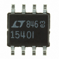
LTC1540IS8#PBF Linear Technology, LTC1540IS8#PBF Datasheet - Page 7

LTC1540IS8#PBF
Manufacturer Part Number
LTC1540IS8#PBF
Description
IC COMP NANOPOWER W/REF 8-SOIC
Manufacturer
Linear Technology
Type
with Voltage Referencer
Datasheet
1.LTC1540CS8PBF.pdf
(12 pages)
Specifications of LTC1540IS8#PBF
Number Of Elements
1
Output Type
CMOS, TTL
Voltage - Supply
2 V ~ 11 V, ±1 V ~ 5.5 V
Mounting Type
Surface Mount
Package / Case
8-SOIC (0.154", 3.90mm Width)
Comparator Type
General Purpose
No. Of Comparators
1
Response Time
50µs
Ic Output Type
CMOS, MOS, Open-Collector / Drain, TTL
Supply Current
300nA
Supply Voltage Range
± 1V To ± 5.5V
Rohs Compliant
Yes
Output Compatibility
CMOS, TTL
Lead Free Status / RoHS Status
Lead free / RoHS Compliant
Available stocks
Company
Part Number
Manufacturer
Quantity
Price
APPLICATIONS
Hysteresis
Hysteresis can be added to the LTC1540 by connecting a
resistor (R1) between the REF and HYST pins and a
second resistor (R2) from HYST to V
The difference between the upper and lower threshold
voltages, or hysteresis voltage band (V
the voltage difference between the REF and HYST pins.
When more hysteresis is added, the upper threshold
increases the same amount as the low threshold de-
creases. The maximum voltage allowed between REF and
HYST pins is 50mV, producing a maximum hysteresis
voltage band of 100mV. The hysteresis band may vary by
Level Detector
The LTC1540 is ideal for use as a nanopower level detector
as shown in Figure 6. R1 and R2 form a voltage divider
from V
set the hysteresis voltage, and R5 and C1 bypass the
reference output. The following design procedure can be
used to select the component values:
1. Choose the V
2. Calculate the required resistive divider ratio.
3. Choose the required hysteresis voltage band at the
4. Choose the values for R3 and R4 to set the hysteresis.
5. Choose the values for R1 and R2 to set the trip point.
TYPICAL APPLICATIONS
Ratio = V
Ratio = 1.182V/4.65V = 0.254
input V
esis voltage band referred to the comparator input V
V
V
V
R4 = 2.4M
R3 (kΩ) = 15k, V
HB
HB
HB
IN
= (V
= (60mV)(0.254)
= 15.24mV
to the noninverting comparator input. R3 and R4
HBIN
HBIN
REF
, in this example 60mV. Calculate the hyster-
/ V
IN
)(Ratio)
IN
voltage trip level, in this example 4.65V.
U
HB
(mV) = 15mV
INFORMATION
U
U
W
HB
–
(Figure 5).
), is equal to twice
U
HB
.
up to 15%. If hysteresis is not wanted, the HYST pin
should be shorted to REF. Acceptable values for I
from 0.1µA to 5µA. If 2.4M is chosen for R2, then the value
of R1 (kΩ) is equal to the value of V
R1 =
R2 = R1
R2 = 1.18M
R2 = 3.40M
V
IN
Figure 6. Glitch-Free Level Detector with Hysteresis
R2
3.4M
1%
R1
1.18M
1%
I
REF
V
I
BIAS
REF
R1
R2
Figure 5. Programmable Hysteresis
R4
2.4M
1%
V
15k
1%
R3
REF
=
1.182V +
6
5
1.182V
V
+
1µA
REF
HYST
IN
R5
430Ω
5%
C1
1µF
V
4.65V
LTC1540
2
HB
3
4
5
6
V
–
2
IN
IN
HYST
REF
= 1.18M
15mV
–
+
– 1
2
V
2
+
–
–
R1 =
R2 =
5V
V
– 1
+
HB
7
(2)(I
(
1.182V –
GND
(mV).
LTC1540
V
HB
1
REF
LTC1540
I
REF
1540 • F05
)
V
2
HB
8
sn1540 1540fas
REF
)
1540 F06
OUT
range
7


