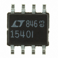
LTC1540IS8#PBF Linear Technology, LTC1540IS8#PBF Datasheet - Page 6

LTC1540IS8#PBF
Manufacturer Part Number
LTC1540IS8#PBF
Description
IC COMP NANOPOWER W/REF 8-SOIC
Manufacturer
Linear Technology
Type
with Voltage Referencer
Datasheet
1.LTC1540CS8PBF.pdf
(12 pages)
Specifications of LTC1540IS8#PBF
Number Of Elements
1
Output Type
CMOS, TTL
Voltage - Supply
2 V ~ 11 V, ±1 V ~ 5.5 V
Mounting Type
Surface Mount
Package / Case
8-SOIC (0.154", 3.90mm Width)
Comparator Type
General Purpose
No. Of Comparators
1
Response Time
50µs
Ic Output Type
CMOS, MOS, Open-Collector / Drain, TTL
Supply Current
300nA
Supply Voltage Range
± 1V To ± 5.5V
Rohs Compliant
Yes
Output Compatibility
CMOS, TTL
Lead Free Status / RoHS Status
Lead free / RoHS Compliant
Available stocks
Company
Part Number
Manufacturer
Quantity
Price
APPLICATIONS
LTC1540
Figure 3 shows the bypassed reference output with a
square wave applied to the V
10mV of hysteresis voltage band while R1 damps the
reference response. Note that the comparator output
doesn’t trip.
Low Voltage Operation: V
The guaranteed minimum operating voltage is 2V (or
±1V). As the total supply voltage is reduced below 2V, the
performance degrades and the supply current falls. At low
supply voltages, the comparator’s output drive is reduced
and the propagation delay increases. The V
also slightly worse. The useful input voltage range extends
from the negative supply to 0.9V below the positive
supply. Test your prototype over the full
temperature and supply voltage range if operation below
2V is anticipated. Because of the increase in supply
current, operation below 1.5V is not recommended
(Figure 4).
6
Figure 2. Damping Resistance vs Bypass Capacitor Value
1000
Figure 1. Damping the Reference Output
100
0.1
10
0.001
1
REFERENCE
OUTPUT
U
0.01
CAPACITOR VALUE (µF)
INFORMATION
R1
U
C1
+
0.1
+
= 1.6V
pin. Resistors R2 and R3 set
REF
V
LTC1540
–
W
1
1540 • F01
1540 • F02
REF
10
and V
U
OS
are
TO
5V
8V
V
Figure 3a. Power Supply Transient Test Circuit
+
V
OUT
Figure 3b. Power Supply Transient Rejection
REF
8V
5V
Figure 4. Supply Current vs Supply Voltage
5
4
3
2
1
0
0
R3
2.4M
V
IN
IN
T
10k
R2
A
–
+
–
= 25°C
= GND = 0V
= 0V
= REF = HYST
0.5
R1
430Ω
SUPPLY VOLTAGE (V)
C1
1µF
1.0
3
4
5
6
2ms/DIV
IN
IN
HYST
REF
+
–
1.5
V
2
+
–
–
V
2.0
+
7
GND
1540 F04
LTC1540
1540 F03b
1
2.5
sn1540 1540fas
8
1540 • F03a
OUT


