CS8420-DSZ Cirrus Logic Inc, CS8420-DSZ Datasheet - Page 53
CS8420-DSZ
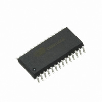
Manufacturer Part Number
CS8420-DSZ
Description
IC CONV S/R DGTL AUDIO 28-SOIC
Manufacturer
Cirrus Logic Inc
Type
Sample Rate Converterr
Datasheet
1.CS8420-CSZ.pdf
(94 pages)
Specifications of CS8420-DSZ
Applications
Digital Audio
Mounting Type
Surface Mount
Package / Case
28-SOIC
Audio Control Type
Sample Rate Converter
Control Interface
3 Wire, Serial
Supply Voltage Range
4.75V To 5.25V
Operating Temperature Range
-40°C To +85°C
Audio Ic Case Style
SOIC
No. Of Pins
28
Lead Free Status / RoHS Status
Lead free / RoHS Compliant
Other names
598-1729
Available stocks
Company
Part Number
Manufacturer
Quantity
Price

Part Number:
CS8420-DSZ
Manufacturer:
CIRRUS
Quantity:
20 000


CS8420
EMPH - Pre-Emphasis Indicator Output
EMPH is low when the incoming AES3 data indicates the presence of 50/15 μs pre-emphasis. When the AES3 data
indicates the absence of pre-emphasis or the presence of other than 50/15 μs pre-emphasis EMPH is high. This is
also a start-up option pin, and requires a 47 kΩ resistor to either VD+ or DGND, which determines the AD2 address
bit for the control port in I²C mode.
Audio Output Interface:
SDOUT - Serial Audio Output Port Data Output
Audio data serial output pin.
OSCLK - Serial Audio Output Port Bit Clock Input or Output
Serial bit clock for audio data on the SDOUT pin.
OLRCK - Serial Audio Output Port Left/Right Clock Input or Output
Word rate clock for the audio data on the SDOUT pin. The frequency will be at the output sample rate (Fso)
AES3/SPDIF Transmitter Interface:
TCBL - Transmit Channel Status Block Start
This pin can be configured as an input or output. When operated as output, TCBL is high during the first sub-frame
of a transmitted channel status block, and low at all other times. When operated as input, driving TCBL high for at
least three OMCK (or RMCK, depending on which clock is operating the AES3 encoder block) clocks will cause the
next transmitted sub-frame to be the start of a channel status block.
TXN, TXP - Differential Line Driver Outputs
Differential line driver outputs, transmitting AES3 type data. Drivers are pulled to low while the CS8420 is in the reset
state.
Control Port Signals:
SCL/CCLK - Control Port Clock
SCL/CCLK is the serial control interface clock, and is used to clock control data bits into and out of the CS8420.
AD0/CS - Address Bit 0 (I²C) / Control Port Chip Select (SPI)
A falling edge on this pin puts the CS8420 into SPI Control Port mode. With no falling edge, the CS8420 defaults to
I²C mode. In I²C mode, AD0 is a chip address pin. In SPI mode, CS is used to enable the control port interface on
the CS8420.
AD1/CDIN - Address Bit 1 (I²C) / Serial Control Data In (SPI)
In I²C mode, AD1 is a chip address pin. In SPI mode, CDIN is the input data line for the control port interface
SDA/CDOUT - Serial Control Data I/O (I²C) / Data Out (SPI)
In I²C mode, SDA is the control I/O data line. SDA is open drain and requires an external pull-up resistor to VD+. In
SPI mode, CDOUT is the output data from the control port interface on the CS8420.
DS245F4
53
Related parts for CS8420-DSZ
Image
Part Number
Description
Manufacturer
Datasheet
Request
R

Part Number:
Description:
IC SAMPLE RATE CONVERTER 28SOIC
Manufacturer:
Cirrus Logic Inc
Datasheet:

Part Number:
Description:
Transceiver IC
Manufacturer:
Cirrus Logic Inc
Datasheet:

Part Number:
Description:
IC,Digital Audio Sample Rate Converter,SOP,28PIN
Manufacturer:
Cirrus Logic Inc
Datasheet:
Part Number:
Description:
IC,Digital Audio Sample Rate Converter,SOP,28PIN
Manufacturer:
Cirrus Logic Inc
Datasheet:
Part Number:
Description:
IC Digital Audio Sample Rate Converter
Manufacturer:
Cirrus Logic Inc

Part Number:
Description:
Audio DSPs IC Digital Audio Sample Rate Convertr
Manufacturer:
Cirrus Logic Inc
Datasheet:
Part Number:
Description:
Audio DSPs IC Digital Audio Sample Rate Convertr
Manufacturer:
Cirrus Logic Inc
Datasheet:

Part Number:
Description:
Development Kit
Manufacturer:
Cirrus Logic Inc
Datasheet:
Part Number:
Description:
Development Kit
Manufacturer:
Cirrus Logic Inc
Datasheet:


Part Number:
Description:
High-efficiency PFC + Fluorescent Lamp Driver Reference Design
Manufacturer:
Cirrus Logic Inc
Datasheet:
Part Number:
Description:
Development Kit
Manufacturer:
Cirrus Logic Inc
Datasheet:
Part Number:
Description:
Development Kit
Manufacturer:
Cirrus Logic Inc
Datasheet:

Part Number:
Description:
Ref Bd For Speakerbar MSA & DSP Products
Manufacturer:
Cirrus Logic Inc