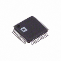
ADAU1701JSTZ Analog Devices Inc, ADAU1701JSTZ Datasheet - Page 5

ADAU1701JSTZ
Manufacturer Part Number
ADAU1701JSTZ
Description
IC AUDIO PROC 2ADC/4DAC 48-LQFP
Manufacturer
Analog Devices Inc
Series
SigmaDSP®r
Type
Audio Processorr
Specifications of ADAU1701JSTZ
Design Resources
Analog Audio Input, Class-D Output with ADAU1701, SSM2306, and ADP3336 (CN0162)
Applications
Automotive, Monitors, MP3
Mounting Type
Surface Mount
Package / Case
48-LQFP
Audio Control Type
Digital
Control Interface
I2C, Serial
Supply Voltage Range
1.8V, 3.3V
Operating Temperature Range
0°C To +70°C
Audio Ic Case Style
LQFP
No. Of Pins
48
Svhc
No SVHC
Control / Process Application
MP3 Player Speaker Docks, Automotive Head Units, Studio Monitors
Rohs Compliant
Yes
Lead Free Status / RoHS Status
Lead free / RoHS Compliant
For Use With
EVAL-ADAU1701MINIZ - BOARD EVAL SIGMADSP AUD ADAU1701EVAL-ADAU1701EBZ - BOARD EVAL FOR ADAU1701
Lead Free Status / RoHS Status
Lead free / RoHS Compliant, Lead free / RoHS Compliant
Available stocks
Company
Part Number
Manufacturer
Quantity
Price
Company:
Part Number:
ADAU1701JSTZ
Manufacturer:
Analog Devices Inc
Quantity:
1 923
Company:
Part Number:
ADAU1701JSTZ
Manufacturer:
ADI
Quantity:
221
Company:
Part Number:
ADAU1701JSTZ
Manufacturer:
Analog Devices Inc
Quantity:
10 000
Part Number:
ADAU1701JSTZ
Manufacturer:
ADI/亚德诺
Quantity:
20 000
Company:
Part Number:
ADAU1701JSTZ-RL
Manufacturer:
ON
Quantity:
35 000
Company:
Part Number:
ADAU1701JSTZ-RL
Manufacturer:
Analog Devices Inc
Quantity:
10 000
Part Number:
ADAU1701JSTZ-RL
Manufacturer:
ADI/亚德诺
Quantity:
20 000
DIGITAL TIMING SPECIFICATIONS
Table 7. Digital Timing
Parameter
MASTER CLOCK
SERIAL PORT
SPI PORT
I
MULTIPURPOSE PINS AND RESET
1
2
All timing specifications are given for the default (I
C PORT
t
t
t
t
t
t
t
t
t
t
t
t
t
t
t
f
t
t
t
t
t
t
t
t
f
t
t
t
t
t
t
t
t
t
t
t
t
t
t
CCLK
SCL
MP
MP
MP
MP
BIL
BIH
LIS
LIH
SIS
SIH
LOS
LOH
TS
SODS
SODM
CCPL
CCPH
CLS
CLH
CLPH
CDS
CDH
COD
SCLH
SCLL
SCS
SCH
DS
SCR
SCF
SDR
SDF
BFT
GRT
GFT
GIL
RLPW
1
T
36
48
73
291
40
40
10
10
10
10
10
10
80
80
0
100
80
0
80
0.6
1.3
0.6
0.6
100
0.6
20
MIN
2
S) states of the serial input port and the serial output port (see Table 66).
Limit
T
244
366
488
1953
5
40
40
6.25
101
400
300
300
300
300
50
50
1.5 × 1/f
MAX
S
Rev. 0 | Page 5 of 52
Unit
ns
ns
ns
ns
ns
ns
ns
ns
ns
ns
ns
ns
ns
ns
ns
MHz
ns
ns
ns
ns
ns
ns
ns
ns
kHz
μs
μs
μs
μs
ns
ns
ns
ns
ns
ns
ns
μs
ns
Description
MCLK period, 512 f
MCLK period, 384 f
MCLK period, 256 f
MCLK period, 64 f
INPUT_BCLK low pulse width.
INPUT_BCLK high pulse width.
INPUT_LRCLK setup. Time to INPUT_BCLK rising.
INPUT_LRCLK hold. Time from INPUT_BCLK rising.
SDATA_INx setup. Time to BCLK_IN rising.
SDATA_INx hold. Time from BCLK_IN rising.
OUTPUT_LRCLK setup in slave mode.
OUTPUT_LRCLK hold in slave mode.
OUTPUT_BCLK falling to OUTPUT_LRCLK timing skew.
SDATA_OUTx delay. Time from OUTPUT_BCLK falling in slave mode.
SDATA_OUTx delay. Time from OUTPUT_BCLK falling in master mode.
CCLK frequency.
CCLK pulse width low.
CCLK pulse width high.
CLATCH setup. Time to CCLK rising.
CLATCH hold. Time from CCLK rising.
CLATCH pulse width high.
CDATA setup. Time to CCLK rising.
CDATA hold. Time from CCLK rising.
COUT delay. Time from CCLK falling.
SCL frequency.
SCL high.
SCL low.
Setup time, relevant for repeated start condition.
Hold time. After this period, the first clock is generated.
Data setup time.
SCL rise time.
SCL fall time.
SDA rise time.
SDA fall time.
Bus-free time. Time between stop and start.
GPIO rise time.
GPIO fall time.
GPIO input latency. Time until high/low value is read by core.
RESET low pulse width.
S
S
S
S
mode.
mode.
mode.
mode.
ADAU1701


