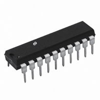
LM2202N National Semiconductor, LM2202N Datasheet - Page 9

LM2202N
Manufacturer Part Number
LM2202N
Description
IC VIDEO AMP SYSTEM 20-DIP
Manufacturer
National Semiconductor
Datasheet
1.LM2202M.pdf
(17 pages)
Specifications of LM2202N
Applications
General Purpose
Number Of Circuits
1
-3db Bandwidth
230MHz
Current - Supply
48mA
Current - Output / Channel
28mA
Voltage - Supply, Single/dual (±)
8 V ~ 13.2 V
Mounting Type
Through Hole
Package / Case
20-DIP (0.300", 7.62mm)
Lead Free Status / RoHS Status
Contains lead / RoHS non-compliant
Other names
*LM2202N
Available stocks
Company
Part Number
Manufacturer
Quantity
Price
Part Number:
LM2202N
Manufacturer:
NS/国半
Quantity:
20 000
Circuit Description
DRIVE CONTROL SECTION
A simplified schematic of the LM2202’s drive control section
is shown in Figure 6 . A 0V to 4V DC voltage is applied at the
drive control input (pin 9). Transistors Q49, Q50 and Q54
buffer and level shift the contrast voltage to the base of Q56.
The voltage at the emitter of Q56 equals the drive voltage,
V
I
Transistor Q56’s collector current is used to unbalance the
current through the differential pair comprised of Q58 and
Q60. Q60’s base is internally biased at 7.3V and connected
to the base of Q12 (see Figure 3 ). Q58’s base is internally
connected to the base of Q11 (see Figure 3 ). With V
2V, the differential pair (Q58, Q60) is balanced and the volt-
age at the bases of Q11 and Q12 is 7.3V. Under this condi-
tion, Q10’s collector current is equally split between Q11 and
Q12 (see Figure 3 ). If the drive voltage at pin 9 is greater
than 2V then Q56’s collector current increases, thus pulling
Q58’s collector node lower and consequently moving Q58’s
base below 7.3V. With base of Q11 below 7.3V, current
through Q12 (see Figure 3 ) increases and the amplifier’s
gain increases. With V
mum under maximum contrast condition (i.e., V
If the drive voltage at pin 8 is less than 2V then Q56’s collec-
tor current decreases and Q58’s base is pulled above 7.3V.
With base of Q11 greater than 7.3V, less current flows
through Q12 (see Figure 3 ), consequently the amplifier’s
gain decreases. With V
less than the maximum gain.
C56
drive
= V
and the current through Q56’s collector is given by
drive
/R43.
drive
drive
= 4V, the amplifier’s gain is maxi-
= 0V, the amplifier’s gain is 6 dB
(Continued)
cont
= 4V).
cont
=
9
CLAMP GATE AND CLAMP COMPARATOR SECTION
Figure 7 and Figure 8 show simplified schematics of the
clamp gate and clamp comparator circuits. The clamp gate
circuit ( Figure 7 ) consists of a PNP input buffer transistor
(Q82), a PNP emitter coupled pair (Q85 and Q86) refer-
enced on one side to 2.1V and an output switch transistor
Q89. When the clamp gate input at pin 14 is high (
the Q89 switch is on and shunts the 200 µA current from cur-
rent source Q90 to ground. When pin 14 is low (
Q89 switch is off and the 200 µA current is mirrored by the
current mirror comprised of Q91 and Q75 (see Figure 8 ).
Consequently the clamp comparator comprised of the differ-
ential pair Q74 and Q77 is enabled. The input of the clamp
comparator is similar to the clamp gate except that an NPN
emitter coupled pair is used to control the current that will
charge or discharge the clamp capacitor externally con-
nected from pin 12 to ground. PNP transistors are used at
the inputs because they offer a number of advantages over
NPNs. PNPs will operate with base voltages at or near
ground and will usually have a greater emitter base break-
down voltage (BVebo). Because the differential input voltage
to the clamp comparator during the video scan period could
be greater than the BVebo of NPN transistors, a resistor
(R63) with a value one half that of R60 or R68 is connected
between the bases of Q71 and Q79. The clamp compara-
tor’s common mode range is from ground to approximately
9V and the maximum differential input voltage is V
www.national.com
<
1.3V) the
CC
>
.
1.5V)


