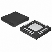
MAX3971AUTP+ Maxim Integrated Products, MAX3971AUTP+ Datasheet - Page 5

MAX3971AUTP+
Manufacturer Part Number
MAX3971AUTP+
Description
IC AMP LIMIT 10.7GBPS 20-TQFN
Manufacturer
Maxim Integrated Products
Type
Limiting Amplifierr
Datasheet
1.MAX3971AUTP.pdf
(9 pages)
Specifications of MAX3971AUTP+
Applications
Optical Networks
Mounting Type
Surface Mount
Package / Case
20-TQFN Exposed Pad
Operating Supply Voltage
3.3 V
Supply Current
50 mA
Operating Temperature Range
+ 85 C
Mounting Style
SMD/SMT
Number Of Channels
1
Power Dissipation
1300 mW
Lead Free Status / RoHS Status
Lead free / RoHS Compliant
Figure 1 is a functional diagram of the MAX3971A limit-
ing amplifier. The signal path consists of an input buffer
followed by a gain stage and output amplifier. A feed-
back loop provides offset correction by driving the
average value of the differential output to zero.
Figure 1. Functional Diagram
5, 7, 9, 10
6, 8, 11
12, 15
PIN
IN-
GNDIN+
IN+
GNDIN-
13
14
16
17
18
19
20
—
1
2
3
4
100Ω
MAX3971A
AMPLIFIER
INPUT
DISABLE
GNDIN+
Detailed Description and
Applications Information
GNDIN-
NAME
OUT+
OUT-
GND
V
V
V
N.C.
CZ+
IN+
CZ-
IN-
EP
_______________________________________________________________________________________
CC3
CC2
CC1
CORRECTION
OFFSET
Input Ground for Shielding Input Signal IN+. Not connected internally.
Noninverting Input Signal
Inverting Input Signal
Input Ground for Shielding Input Signal IN-. Not connected internally.
No Connection. Leave unconnected.
Ground
Output Circuitry Power Supply
Inverting Output of Amplifier
Noninverting Output of Amplifier
When DISABLE is connected to V
connected to GND, outputs are enabled.
Power Supply to Circuitry other than Input and Output Circuits
Filter Capacitor for Offset Correction. Connect CZ between pin 18 and pin 19. See the Detailed
Description section.
Filter Capacitor for Offset Correction. Connect CZ between pin 18 and pin 19. See the Detailed
Description section.
Input Circuitry Power Supply
Exposed Pad. Must be soldered to supply ground for proper electrical and thermal operation.
AMP
GAIN
42dB
+3.3V, 10.7Gbps Limiting Amplifier
CZ-
LOWPASS
FILTER
CZ
CZ+
AMPLIFIER
OUTPUT
DISABLE
OUT+
OUT-
CC
or left floating, outputs are disabled. When DISABLE is
The limiting amplifier provides approximately 42dB
gain. The large gain makes the amplifier susceptible to
small DC offsets, which cause deterministic jitter. A
low-frequency loop is integrated into the limiting ampli-
fier to reduce output offset, typically to less than 2mV.
The external capacitor (CZ) is required for stability and
to set the low-frequency cutoff for the offset correction
loop. The time constant of the loop is set by the product
of an equivalent 20kΩ on-chip resistor and the value of
the off-chip capacitor (CZ). For stable operation, the
minimum value of CZ is 0.01µF. To minimize pattern-
dependent jitter, CZ should be as large as possible.
For 10Gbps ethernet and SONET applications, the typi-
cal value of CZ is 0.1µF. Keep CZ close to the package
to reduce parasitic inductance.
The input buffer is designed to accept CML input sig-
nals such as the output from the MAX3970 transimped-
ance amplifier. An equivalent circuit for the input is
shown in Figure 2. For lowest deterministic jitter in all
operating conditions, AC-coupling capacitors are rec-
ommended on the input.
FUNCTION
Gain Stage and Offset Correction
Pin Description
CML Input Circuit
5


