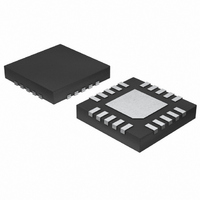
MAX3971AUTP+ Maxim Integrated Products, MAX3971AUTP+ Datasheet

MAX3971AUTP+
Specifications of MAX3971AUTP+
Related parts for MAX3971AUTP+
MAX3971AUTP+ Summary of contents
Page 1
... Typical Deterministic Jitter (V ♦ Dice and 4mm × 4mm QFN or Thin QFN Package Available ♦ Output Disable Feature Applications PART MAX3971AUGP MAX3971AUTP MAX3971AUTP+ MAX3971AU Exposed pad. ** Dice are designed to operate over a 0°C to +110°C junction- temperature ( +25° Denotes lead-free package. ...
Page 2
Limiting Amplifier ABSOLUTE MAXIMUM RATINGS Supply Voltage ......................-0.5V to +5.0 V CC1 CC2 CC3 Voltage at IN+, IN-, DISABLE, CZ+, CZ-, OUT+, OUT- .........................................+0. Differential Voltage Between CZ+ and CZ- ...........................±1V ...
Page 3
Limiting Amplifier (V = +3.3V, output load = 50Ω OUTPUT EYE DIAGRAM (INPUT SIGNAL = 10mV , AT 10.7Gbps) P 1PRBS 45mV/div 20ps/div OUTPUT EYE DIAGRAM (INPUT SIGNAL = 800mV , ...
Page 4
Limiting Amplifier (V = +3.3V, output load = 50Ω DETERMINISTIC JITTER vs. TEMPERATURE 7 10.7Gbps with K28 5mV 800mV ...
Page 5
Limiting Amplifier PIN NAME 1 GNDIN+ Input Ground for Shielding Input Signal IN+. Not connected internally. 2 IN+ Noninverting Input Signal 3 IN- Inverting Input Signal 4 GNDIN- Input Ground for Shielding Input Signal IN-. Not connected internally. ...
Page 6
Limiting Amplifier V CC1 GNDIN+ 50Ω 50Ω IN+ IN- GNDIN- ESD STRUCTURES Figure 2. CML Input Equivalent Circuit V CC3 50Ω 50Ω DISABLE DATA Figure 3. CML Output Equivalent Circuit CML Output Circuit An ...
Page 7
Limiting Amplifier Layout Considerations Circuit board layout and design can significantly affect the performance of the MAX3971A. Use good high-fre- quency techniques, including fixed-impedance trans- mission lines for the high-frequency data signal. Use a multilayer board with solid ...
Page 8
Limiting Amplifier GNDIN+ IN+ IN- GNDIN- NC (0, 0) GND 8 _______________________________________________________________________________________ V CZ- CZ+ V CC1 CC2 N.C. GND N.C. N.C. 0.042" (1.10mm) Chip Topography DISABLE V CC3 OUT+ OUT- 0.052" (1.33mm) V CC3 GND ...
Page 9
... Maxim cannot assume responsibility for use of any circuitry other than circuitry entirely embodied in a Maxim product. No circuit patent licenses are implied. Maxim reserves the right to change the circuitry and specifications without notice at any time. Maxim Integrated Products, 120 San Gabriel Drive, Sunnyvale, CA 94086 408-737-7600 _____________________ 9 © 2007 Maxim Integrated Products Chip Topography (continued) • ...


