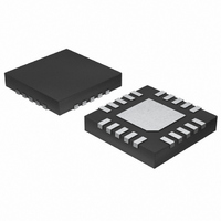
MAX3971AUTP+ Maxim Integrated Products, MAX3971AUTP+ Datasheet - Page 2

MAX3971AUTP+
Manufacturer Part Number
MAX3971AUTP+
Description
IC AMP LIMIT 10.7GBPS 20-TQFN
Manufacturer
Maxim Integrated Products
Type
Limiting Amplifierr
Datasheet
1.MAX3971AUTP.pdf
(9 pages)
Specifications of MAX3971AUTP+
Applications
Optical Networks
Mounting Type
Surface Mount
Package / Case
20-TQFN Exposed Pad
Operating Supply Voltage
3.3 V
Supply Current
50 mA
Operating Temperature Range
+ 85 C
Mounting Style
SMD/SMT
Number Of Channels
1
Power Dissipation
1300 mW
Lead Free Status / RoHS Status
Lead free / RoHS Compliant
ELECTRICAL CHARACTERISTICS
(V
a 2
+3.3V, 10.7Gbps Limiting Amplifier
ABSOLUTE MAXIMUM RATINGS
Supply Voltage, V
Voltage at IN+, IN-, DISABLE, CZ+, CZ-,
Differential Voltage Between CZ+ and CZ- ...........................±1V
Differential Voltage Between IN+ and IN-...........................±2.5V
Continuous Power Dissipation (T
Stresses beyond those listed under “Absolute Maximum Ratings” may cause permanent damage to the device. These are stress ratings only, and functional
operation of the device at these or any other conditions beyond those indicated in the operational sections of the specifications is not implied. Exposure to
absolute maximum rating conditions for extended periods may affect device reliability.
Note 1: Guaranteed by design and characterization.
Note 2: The output signal amplitude at the sensitivity is > .95
Note 3: Deterministic jitter is measured with K28.5 pattern (0011 1110 1011 0000 0101) at 10.7Gbps. It is the peak-to-peak devia-
Note 4: For a bit-error rate of 10
2
PARAMETER
Supply Current
Small-Signal Bandwidth
Input Sensitivity
Input Overload
Low-Frequency Cutoff
Deterministic Jitter
Random Jitter
Transition Time
Data Input Impedance
Data Output-Voltage Swing
Data Output Voltage when
Disabled
Data Output Common-Mode
Voltage
Data Output Impedance
Data Output Offset when
DISABLE is High
Disable Input Current
DISABLE High Voltage
DISABLE Low Voltage
Disable Response Time
CC
23
OUT+, OUT- .........................................+0.5V to (V
20-Pin QFN (derate 20mW/°C above +85°C) .................1.3W
_______________________________________________________________________________________
= +3.0V to +3.6V, output load = 50Ω to V
- 1 PRBS pattern applied to the input at 10.7Gbps. Typical values are at V
tion from the ideal time crossing, measured at the zero-level crossing of the differential output.
CC1
, V
CC2
, V
CC3
A
-12
= +85°C)
......................-0.5V to +5.0 V
, the peak-to-peak random jitter is 14.1
SYMBOL
V
V
IN-max
IN-min
I
BW
t
V
V
CC
r
, t
IH
IL
f
CC
, T
(Notes 1, 2)
(Note 1)
CZ = 0.1µF (Note 1)
5mV
10mV
800mV
1200mV
20mV
20% to 80%, differential output (Note 1)
Single ended
Differential signal amplitude between
OUT+ and OUT-
Differential signal amplitude
between OUT+ and OUT-
Single ended
A
CC
= 0°C to +85°C, unless otherwise noted. All AC parameters are measured with
P-P
P-P
P-P
+ 0.5V)
P-P
input (Notes 1, 3)
P-P
input (Notes 1, 3)
< input < 1200mV
input (Notes 1, 3)
input (Notes 1, 3)
✕
the amplitude with large input.
CONDITIONS
Operating Ambient Temperature Range .............-40°C to +85°C
Storage Temperature Range .............................-55°C to +150°C
Die Attach Temperature...................................................+400°C
Lead Temperature (soldering, 10s) .................................+300°C
✕
the RMS random jitter.
P-P
CC
(Notes 1, 4)
= +3.3V, T
A
= +25°C, unless otherwise noted.)
1200
MIN
190
42
42
2
V
TYP
0.25
240
5.2
3.5
1.8
1.9
0.6
CC
50
10
60
20
50
75
50
75
30
20
2
-
MAX
16.0
14.0
11.0
400
200
7.0
1.1
0.8
85
75
30
58
50
58
60
5
UNITS
ps
mV
mV
mV
mV
GHz
kHz
mA
mV
mV
ps
µA
ps
ns
Ω
Ω
RMS
V
V
P-P
P-P
P-P
P-P


