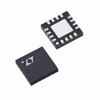
LTC6400CUD-14#PBF Linear Technology, LTC6400CUD-14#PBF Datasheet - Page 3

LTC6400CUD-14#PBF
Manufacturer Part Number
LTC6400CUD-14#PBF
Description
IC ADC DRIVER DIFF 16-QFN
Manufacturer
Linear Technology
Type
ADC Driverr
Datasheet
1.LTC6400CUD-14PBF.pdf
(16 pages)
Specifications of LTC6400CUD-14#PBF
Applications
Data Acquisition
Mounting Type
Surface Mount
Package / Case
16-WQFN Exposed Pad
No. Of Amplifiers
1
Input Offset Voltage
3mV
Gain Db Max
14dB
Bandwidth
2.4GHz
Slew Rate
4800V/µs
Supply Voltage Range
2.85V To 3.5V
Supply Current
85mA
Amplifier Case Style
QFN
Rohs Compliant
Yes
Lead Free Status / RoHS Status
Lead free / RoHS Compliant
Available stocks
Company
Part Number
Manufacturer
Quantity
Price
DC ELECTRICAL CHARACTERISTICS
temperature range, otherwise specifi cations are at T
otherwise noted.
SYMBOL
Input/Output Characteristic
G
TC
V
V
V
I
V
TCV
I
I
R
C
R
R
C
CMRR
Output Common Mode Voltage Control
G
V
V
V
TCV
IV
ENABLE Pin
V
V
I
I
Power Supply
V
I
I
PSRR
OUT
VRMIN
VRMAX
IL
IH
S
SHDN
SWINGMIN
SWINGMAX
OUTDIFFMAX
OSDIFF
INDIFF
OUTFDIFF
OCMMIN
OCMMAX
OSCM
IL
IH
S
DIFF
INDIFF
OUTDIFF
OUTFDIFF
CM
OCM
GAIN
OSDIFF
OSCM
PARAMETER
Gain
Gain Temperature Drift
Output Swing Low
Output Swing High
Maximum Differential Output Swing
Output Current Drive
Input Differential Offset Voltage
Input Differential Offset Voltage Drift
Input Common Mode Voltage Range, MIN
Input Common Mode Voltage Range, MAX
Input Resistance (+IN, –IN)
Input Capacitance (+IN, –IN)
Output Resistance (+OUT, –OUT)
Filtered Output Resistance (+OUTF, –OUTF)
Filtered Output Capacitance (+OUTF, –OUTF)
Common Mode Rejection Ratio
Common Mode Gain
Output Common Mode Range, MIN
Output Common Mode Range, MAX
Common Mode Offset Voltage
Common Mode Offset Voltage Drift
V
ENABLE Input Low Voltage
ENABLE Input High Voltage
ENABLE Input Low Current
ENABLE Input High Current
Operating Supply Range
Supply Current
Shutdown Supply Current
Power Supply Rejection Ratio (Differential
Outputs)
OCM
Input Current
A
= 25°C. V
CONDITIONS
V
V
Each Output, V
Each Output, V
1dB Compressed
Each Output
T
Differential
Differential, Includes Parasitic
Differential
Differential
Differential, Includes Parasitic
Input Common Mode Voltage 1.1V~1.7V
V
V
T
ENABLE = 0.8V
ENABLE = 2.4V
ENABLE = 0.8V
ENABLE = 2.4V, Input and Output Floating
V
IN
IN
MIN
OCM
OCM
MIN
+
= 2.85V to 3.5V
= ±200mV Differential
= ±200mV Differential
to T
to T
= 1V to 1.6V
= 1.1V to 1.5V
+
= 3V, V
MAX
MAX
The
l
IN
IN
–
denotes the specifi cations which apply over the full operating
= ±800mV Differential
= ±800mV Differential
= 0V, +IN = –IN = V
OCM
l
l
l
l
l
l
l
l
l
l
l
l
l
l
l
l
l
l
l
l
l
l
l
l
l
= 1.25V, ENABLE = 0V, No R
13.5
2.35
2.85
MIN
170
–15
1.8
1.6
1.5
2.4
20
–3
18
85
40
70
55
LTC6400-14
–0.9
2.48
TYP
200
100
4.8
0.7
2.7
1.3
0.9
14
77
25
62
85
76
1
1
9
4
3
MAX
14.5
160
230
115
1.1
0.8
0.5
3.5
32
15
15
96
3
1
1
3
3
L
unless
mdB/°C
640014fb
UNITS
μV/°C
μV/°C
3
V
V/V
mV
mA
mV
mV
mA
mA
P-P
dB
dB
μA
μA
μA
dB
pF
pF
Ω
Ω
Ω
V
V
V
V
V
V
V
V
V
V


