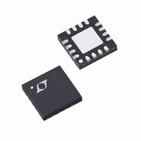
LTC6400CUD-14#PBF Linear Technology, LTC6400CUD-14#PBF Datasheet - Page 11

LTC6400CUD-14#PBF
Manufacturer Part Number
LTC6400CUD-14#PBF
Description
IC ADC DRIVER DIFF 16-QFN
Manufacturer
Linear Technology
Type
ADC Driverr
Datasheet
1.LTC6400CUD-14PBF.pdf
(16 pages)
Specifications of LTC6400CUD-14#PBF
Applications
Data Acquisition
Mounting Type
Surface Mount
Package / Case
16-WQFN Exposed Pad
No. Of Amplifiers
1
Input Offset Voltage
3mV
Gain Db Max
14dB
Bandwidth
2.4GHz
Slew Rate
4800V/µs
Supply Voltage Range
2.85V To 3.5V
Supply Current
85mA
Amplifier Case Style
QFN
Rohs Compliant
Yes
Lead Free Status / RoHS Status
Lead free / RoHS Compliant
Available stocks
Company
Part Number
Manufacturer
Quantity
Price
APPLICATIONS INFORMATION
Circuit Operation
The LTC6400-14 is a low noise and low distortion fully
differential op amp/ADC driver with:
The LTC6400 is composed of a fully differential amplifi er
with on chip feedback and output common mode voltage
control circuitry. Differential gain and input impedance are
set by 100Ω/1000Ω resistors in the feedback network.
Small output resistors of 12.5Ω improve the circuit stability
over various load conditions. They also provide a possible
external fi ltering option, which is often desirable when the
load is an ADC.
Filter resistors of 50Ω are available for additional fi ltering.
Lowpass/bandpass fi lters are easily implemented with
just a couple of external components. Moreover, they of-
fer single-ended 50Ω matching in wideband applications
and no external resistor is needed.
The LTC6400-14 is very fl exible in terms of I/O coupling.
It can be AC- or DC-coupled at the inputs, the outputs or
both. Due to the internal connection between input and
output, users are advised to keep input common mode
voltage between 1V and 1.8V for proper operation. If the
inputs are AC-coupled, the input common mode voltage
is automatically biased approximately 450mV above V
and thus no external circuitry is needed for bias. The
LTC6400-14 provides an output common mode voltage
set by V
external components such as a transformer or AC coupling
capacitors. The input signal can be either single-ended
or differential with only minor differences in distortion
performance.
Input Impedance and Matching
The differential input impedance of the LTC6400-14 is
200Ω. If a 200Ω source impedance is unavailable, then
the differential inputs may need to be terminated to a lower
• Operation from DC to 2.4GHz (–3dB bandwidth)
• Fixed gain of 5V/V (14dB)
• Differential input impedance 200Ω
• Differential output impedance 25Ω
• On-Chip 590MHz output fi lter
OCM
, which allows driving an ADC directly without
OCM
MINI-CIRCUITS
value impedance, e.g. 50Ω, in order to provide an imped-
ance match for the source. Several choices are available.
One approach is to use a differential shunt resistor (Figure
1). Another approach is to employ a wide band transformer
(Figure 2). Both methods provide a wide band impedance
match. The termination resistor or the transformer must
be placed close to the input pins in order to minimize
the refl ection due to input mismatch. Alternatively, one
could apply a narrowband impedance match at the inputs
of the LTC6400-14 for frequency selection and/or noise
reduction.
Referring to Figure 3, LTC6400-14 can be easily confi gured
for single-ended input and differential output without a
balun. The signal is fed to one of the inputs through a
matching network while the other input is connected to the
same matching network and a source resistor. Because the
return ratios of the two feedback paths are equal, the two
outputs have the same gain and thus symmetrical swing.
Figure 1. Input Termination for Differential 50Ω Input Impedance
Using Shunt Resistor
Figure 2. Input Termination for Differential 50Ω Input Impedance
Using a 1:4 Balun
+
–
+
–
TCM4-19
V
25Ω
25Ω
V
25Ω
25Ω
IN
IN
•
1:4
66.5Ω
•
13
14
15
16
13
14
15
16
+IN
+IN
–IN
–IN
+IN
+IN
–IN
–IN
100Ω
100Ω
100Ω
100Ω
IN+
IN–
IN+
IN–
500Ω
500Ω
500Ω
500Ω
OUT–
OUT+
OUT–
OUT+
LTC6400-14
12.5Ω
12.5Ω
12.5Ω
12.5Ω
50Ω
50Ω
50Ω
50Ω
LTC6400-14
LTC6400-14
2.7pF
2.7pF
11
+OUTF
–OUTF
+OUTF
–OUTF
640014 F01
640014 F02
+OUT
–OUT
+OUT
–OUT
640014fb
8
7
6
5
8
7
6
5


