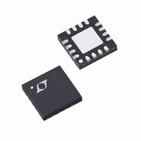
LTC6400CUD-8#PBF Linear Technology, LTC6400CUD-8#PBF Datasheet

LTC6400CUD-8#PBF
Specifications of LTC6400CUD-8#PBF
Available stocks
Related parts for LTC6400CUD-8#PBF
LTC6400CUD-8#PBF Summary of contents
Page 1
... The LTC6400-8 is packaged in a compact 16-lead 3mm × 3mm QFN package and operates over the –40°C to 85°C temperature range. L, LT, LTC and LTM are registered trademarks of Linear Technology Corporation. All other trademarks are the property of their respective owners. 3.3V ...
Page 2
... Storage Temperature Range ................... –65°C to 150°C Maximum Junction Temperature........................... 150°C ORDER INFORMATION LEAD FREE FINISH TAPE AND REEL LTC6400CUD-8#PBF LTC6400CUD-8#TRPBF LTC6400IUD-8#PBF LTC6400IUD-8#TRPBF Consult LTC Marketing for parts specifi ed with wider operating temperature ranges. *The temperature grade is identifi label on the shipping container. ...
Page 3
DC ELECTRICAL CHARACTERISTICS temperature range, otherwise specifi cations are at T otherwise noted. SYMBOL PARAMETER Input/Output Characteristic G Gain DIFF TC Gain Temperature Drift GAIN V Output Swing Low SWINGMIN V Output Swing High SWINGMAX V Maximum Differential Output Swing ...
Page 4
LTC6400-8 AC ELECTRICAL CHARACTERISTICS ENABLE = 0V unless otherwise noted. L SYMBOL PARAMETER –3dBBW –3dB Bandwidth 0.5dBBW Bandwidth for 0.5dB Flatness 0.1dBBW Bandwidth for 0.1dB Flatness 1/f 1/f Noise Corner SR Slew Rate t 1% Settling Time S1% ...
Page 5
AC ELECTRICAL CHARACTERISTICS ENABLE = 0V unless otherwise noted. L SYMBOL PARAMETER P1dB,140M 1dB Compression Point NF140M Noise Figure e Input Referred Voltage Noise Density IN,140M e Output Referred Voltage Noise Density ON,140M 240MHz Input Signal HD2,240M/ Second-Order ...
Page 6
LTC6400-8 TYPICAL PERFORMANCE CHARACTERISTICS Frequency Response 14 TEST CIRCUIT –2 –4 10 100 1000 3000 FREQUENCY (MHz) 64008 G01 Input and Output Refl ection and Reverse Isolation vs Frequency 0 TEST CIRCUIT ...
Page 7
TYPICAL PERFORMANCE CHARACTERISTICS Overdrive Recovery Response 87.5Ω PER OUTPUT L TEST CIRCUIT – +IN 0 +OUT –1 –2 –3 –4 –OUT – 100 120 140 160 180 ...
Page 8
LTC6400-8 TYPICAL PERFORMANCE CHARACTERISTICS Turn-On Time 3.5 3.0 2.5 2.0 +OUT 1.5 –OUT 1.0 0 87.5Ω PER OUTPUT L –0.5 – TIME (ns) PIN FUNCTIONS + V (Pins 1, 3, 10): Positive Power Supply (Normally ...
Page 9
BLOCK DIAGRAM APPLICATIONS INFORMATION Circuit Operation The LTC6400 low noise and low distortion fully differential op amp/ADC driver with: • Operation from DC to 2.2GHz –3dB bandwidth • Fixed gain of 2.5V/V (8dB) • Differential input impedance 400Ω ...
Page 10
LTC6400-8 APPLICATIONS INFORMATION 25Ω 200Ω 500Ω 13 +IN IN+ OUT– +IN + 57.6Ω – 15 –IN IN– OUT+ 25Ω 200Ω 500Ω 16 –IN Figure 1. Input Termination for Differential 50Ω Input Impedance Using Shunt Resistor 500Ω 25Ω ...
Page 11
APPLICATIONS INFORMATION Output Impedance Match and Filter The LTC6400-8 can drive an ADC directly without external output impedance matching. Alternatively, the differential output impedance of 25Ω can be made larger, e.g. 50Ω, by series resistors or LC network. The internal ...
Page 12
LTC6400-8 APPLICATIONS INFORMATION Figure 8 summarizes the IMD3 performance of the whole system as shown in Figure 7. –40 SINGLE-ENDED INPUT F = 122.8Msps S –50 DRIVER COMPOSITE OUT P-P –60 –70 –80 –90 –100 –110 0 ...
Page 13
... C7 0.1μF C23 C5 0.1μF 0.1μF R21 R22 (1) (1) C24 C6 0.1μF 0.1μ LTC6400CUD-8 200Ω MINI-CIRCUITS TCM4-19 (1:4) LTC6400-8 C18 0.1μF R10 R14 86.6Ω (1) R12 TCM 4: (1) 0.1μF 1:4 2 SL2 R7 R11 ...
Page 14
LTC6400-8 TYPICAL APPLICATIONS PORT 1 (50Ω) 0.1μF 1/2 AGILENT 133Ω E5O71A PORT 2 (50Ω) 0.1μF 14 Test Circuit B, 4-Port Analysis + V 1000pF 0.1μF V – ENABLE + BIAS CONTROL ...
Page 15
... ON THE TOP AND BOTTOM OF PACKAGE Information furnished by Linear Technology Corporation is believed to be accurate and reliable. However, no responsibility is assumed for its use. Linear Technology Corporation makes no representa- tion that the interconnection of its circuits as described herein will not infringe on existing patent rights. UD Package 16-Lead Plastic QFN (3mm × ...
Page 16
... SNR = 86dB at 3V Supply, 4th Order Filter SNR = 82dB at 3V Supply, 4th Order Filter SNR = 82dB at 3V Supply, 4th Order Filter SNR = 76dB at 3V Supply, 4th Order Filter SNR = 76dB at 3V Supply, 4th Order Filter l www.linear.com = 1, – 64008f LT 0708 • PRINTED IN USA © LINEAR TECHNOLOGY CORPORATION 2008 ...


