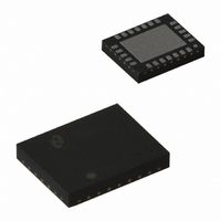
LM4804LQX/NOPB National Semiconductor, LM4804LQX/NOPB Datasheet - Page 3

LM4804LQX/NOPB
Manufacturer Part Number
LM4804LQX/NOPB
Description
IC AMP AUDIO PWR 1.9W MONO 28LLP
Manufacturer
National Semiconductor
Series
Boomer®r
Type
Class ABr
Datasheet
1.LM4804LQNOPB.pdf
(17 pages)
Specifications of LM4804LQX/NOPB
Output Type
1-Channel (Mono)
Max Output Power X Channels @ Load
1.9W x 1 @ 8 Ohm
Voltage - Supply
2.7 V ~ 6.1 V
Features
Depop, Short-Circuit and Thermal Protection, Shutdown
Mounting Type
Surface Mount
Package / Case
28-LLP
Operational Class
Class-AB
Audio Amplifier Output Configuration
1-Channel Mono
Output Power (typ)
1.9x1@8OhmW
Audio Amplifier Function
Speaker
Total Harmonic Distortion
0.13@8Ohm@1.5W%
Single Supply Voltage (typ)
Not RequiredV
Dual Supply Voltage (typ)
3/5V
Power Supply Requirement
Dual
Power Dissipation
1.8W
Rail/rail I/o Type
No
Power Supply Rejection Ratio
72dB
Single Supply Voltage (min)
Not RequiredV
Single Supply Voltage (max)
Not RequiredV
Dual Supply Voltage (min)
2.7/3V
Dual Supply Voltage (max)
5/6.1V
Operating Temp Range
-40C to 85C
Operating Temperature Classification
Industrial
Mounting
Surface Mount
Pin Count
28
Package Type
LLP EP
Lead Free Status / RoHS Status
Lead free / RoHS Compliant
I
I
V
V
T
V
TSD
P
THD+N
e
PSRR
V
I
I
V
V
T
V
DD
SD
DD
SD
OS
WU
WU
SDIH
SDIL
OS
OUT
FB
SDIH
SDIL
OS
Absolute Maximum Ratings
If Military/Aerospace specified devices are required,
please contact the National Semiconductor Sales Office/
Distributors for availability and specifications.
Electrical Characteristics V
The following specifications apply for V
= 78.7kΩ unless otherwise specified. Limits apply for T
Electrical Characteristics V
The following specifications apply for V
= 78.7kΩ unless otherwise specified. Limits apply for T
Supply Voltage (V
Supply Voltage (V
Storage Temperature
Input Voltage
Power Dissipation (Note 3)
ESD Susceptibility (Note 4)
ESD Susceptibility (Note 5)
Symbol
Symbol
Quiescent Power Supply Current
Shutdown Current
Shutdown Voltage Input High
Shutdown Voltage Input Low
Wake-up Time
Output Offset Voltage
Thermal Shutdown Temperature
Output Power
Total Harmomic Distortion + Noise
Output Noise
Power Supply Rejection Ratio
Feedback Pin Reference Voltage
Quiescent Power Supply Current
Shutdown Current
Shutdown Voltage Input High
Shutdown Voltage Input Low
Wake-up Time
Output Offset Voltage
DD
1
)
)
Parameter
Parameter
−0.3V to V
DD
DD
−65˚C to +150˚C
Internally limited
= 4.2V, V
= 3.0V, V
DD
DD
(Notes 1, 2)
DD
= 4.2V
= 3.0V
+ 0.3V
1
1
2000V
200V
= 6.0V, A
= 6.0V, A
6.5V
6.5V
V
V
SD1
SD2
SD1
SD2
C
THD = 2% (max)
P
A-Weighted Filter, V
Input Referred
V
f = 217Hz
f = 1kHz
V
V
SD1
SD2
SD1
SD2
C
A
A
IN
SHUTDOWN
OUT
RIPPLE
DD
SHUTDOWN
B
B
= 25˚C. See Figure 1.
= 25˚C.
= 1.0µF
= 1.0µF
= 0, R
= 3.2V, V
= 1.5W
(Notes 1, 2)
(Notes 1, 2)
= 200mV
3
V-BTL
V-BTL
LOAD
Conditions
Conditions
= GND (Notes 9, 10)
= GND (Notes 9, 10)
Operating Ratings
Junction Temperature
Thermal Resistance
See AN-1187 ’Leadless Leadframe Packaging (LLP).’
Temperature Range
Supply Voltage (V
Supply Voltage (V
IN
= 20dB, R
= 20dB, R
=
θ
T
= 0, R
JA
MIN
p-p
∞
(LLP)
IN
≤ T
= 0V,
LOAD
A
L
L
≤ T
= 8Ω, f
= 8Ω, f
=
MAX
∞
DD
1
)
IN
IN
)
= 1kHz, C
= 1kHz, C
(Note 6)
(Note 6)
Typical
Typical
0.13
1.24
0.1
1.9
0.1
11
70
22
72
67
19
70
4
3
LM4804
LM4804
B
B
= 1.0µF, R
= 1.0µF, R
(Notes 7, 8)
(Notes 7, 8)
−40˚C ≤ T
0.15V
0.15V
0.7V
0.7V
1.2772
1.2028
Limit
Limit
125
1.4
0.4
1.7
0.5
1.4
0.4
2.7V ≤ V
22
40
33
40
2
2
3V ≤ V
DD
DD
DD
DD
1
1
= 301kΩ, R
= 301kΩ, R
www.national.com
A
1
≤ +85˚C
DD
59˚C/W
mA (max)
mV (max)
mA (max)
mV (max)
µA (max)
µA (max)
dB (min)
˚C (min)
≤ 6.1V
(Limits)
V (max)
W (min)
V (max)
(Limits)
V (max)
V (min)
V (min)
V (min)
125˚C
(max)
(max)
Units
msec
Units
msec
≤ 5V
µV
%
2
2


