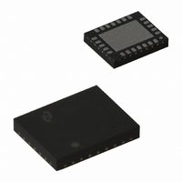
LM4804LQX/NOPB National Semiconductor, LM4804LQX/NOPB Datasheet

LM4804LQX/NOPB
Specifications of LM4804LQX/NOPB
Related parts for LM4804LQX/NOPB
LM4804LQX/NOPB Summary of contents
Page 1
... The LM4804 is unity-gain stable. Its closed-loop gain is determined by the value of external, user selected resistors. Connection Diagrams LM4804LQ (5x5) Top View Order Number LM4804LQ See NS Package Number LQA28A Boomer ® registered trademark of National Semiconductor Corporation. © 2005 National Semiconductor Corporation Key Specifications j Quiescent Power Supply Current (V = 4.2V ...
Page 2
Typical Application FIGURE 1. Typical LM4804 Audio Amplifier Application Circuit www.national.com 20116714 2 ...
Page 3
... Absolute Maximum Ratings If Military/Aerospace specified devices are required, please contact the National Semiconductor Sales Office/ Distributors for availability and specifications. Supply Voltage ( Supply Voltage ( Storage Temperature Input Voltage Power Dissipation (Note 3) ESD Susceptibility (Note 4) ESD Susceptibility (Note 5) Electrical Characteristics V The following specifications apply for V = 78.7kΩ ...
Page 4
Electrical Characteristics V The following specifications apply for V = 78.7kΩ unless otherwise specified. Limits apply for T Symbol Parameter TSD Thermal Shutdown Temperature P Output Power OUT THD+N Total Harmomic Distortion + Noise e Output Noise OS PSRR Power ...
Page 5
Typical Performance Characteristics THD+N vs Frequency V = 4.2V 8Ω OUT THD+N vs Output Power V = 4.2V 8Ω 1kHz DD L PSRR vs Frequency V = 3V, Input Referred DD ...
Page 6
Typical Performance Characteristics Power Supply Current vs Power Supply Voltage R = 8Ω L Output Power vs Power Supply Voltage R = 8Ω L Efficiency 5.0V OUT www.national.com (Continued) 20116727 20116729 IN 20116731 6 Power Supply ...
Page 7
Typical Performance Characteristics Frequency Typical R DS(ON) vs Temperature (Continued) Maximum Start Up Voltage 20116733 Typical Current Limit 20116735 7 vs Temperature 20116734 vs Temperature 20116736 www.national.com ...
Page 8
... This plane forms a thermal mass, heat sink, and radiation area. Further detailed and specific information concerning PCB layout, fabrication, and mounting an LD (LLP) package is available from National Semiconductor’s Package Engineering Group under application note AN1187. SHUTDOWN FUNCTION In many applications, a microcontroller or microprocessor 2 / (2π ...
Page 9
Application Information EXTERNAL COMPONENT SELECTION Proper selection of external components in applications us- ing integrated power amplifiers, and switching DC-DC con- verters, is critical to optimize device and system perfor- mance. Consideration to component values must be used to maximize ...
Page 10
Application Information FIGURE 2. Functional Diagram of the LM4804’s Regulator GATED OSCILLATOR CONTROL SCHEME The on/off regulation mode of the LM4804, along with its ultra-low quiescent current, results in good efficiency over a very wide load range. The internal oscillator ...
Page 11
Application Information PULSE FREQUENCY MODULATION (PFM) Pulse Frequency Modulation is typically accomplished by switching continuously until the voltage limit is reached and skipping cycles after that to just maintain it. This results in a somewhat hysteretic mode of operation. The ...
Page 12
Application Information A value of 50k to 100k is suggested for R selected using the above equation. V SUPPLY DD The Vdd supply must be between volts for the LM4804. This voltage can be bootstrapped from a ...
Page 13
Application Information (Continued) FIGURE 4. Demo Board Reference Schematic 13 20116714 www.national.com ...
Page 14
Demonstration Board Layout FIGURE 5. Top Trace Layer Silkscreen FIGURE 7. Top Trace Layer www.national.com 20116720 FIGURE 6. Top Layer Silkscreen 20116719 FIGURE 8. Upper Internal GND Layer 14 20116718 20116716 ...
Page 15
Demonstration Board Layout FIGURE 9. Lower Internal V (Continued) 20116717 Layer FIGURE 10. Bottom Trace Layer with GND Plane DD 15 20116715 www.national.com ...
Page 16
Revision History Rev 1.0 6/14/05 www.national.com Date Under SHUTDOWN (Apps section), changed EN to S/D1 and (pin– 2) into pin 26, then re-released D/S to the WEB. 16 Description ...
Page 17
... BANNED SUBSTANCE COMPLIANCE National Semiconductor manufactures products and uses packing materials that meet the provisions of the Customer Products Stewardship Specification (CSP-9-111C2) and the Banned Substances and Materials of Interest Specification (CSP-9-111S2) and contain no ‘‘Banned Substances’’ as defined in CSP-9-111S2. ...


