SA58672TK,138 NXP Semiconductors, SA58672TK,138 Datasheet - Page 24
SA58672TK,138
Manufacturer Part Number
SA58672TK,138
Description
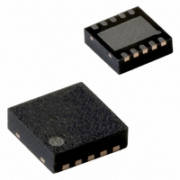
IC AMP AUDIO 3W MONO D 10HVSON
Manufacturer
NXP Semiconductors
Type
Class Dr
Datasheet
1.SA58672UK027.pdf
(27 pages)
Specifications of SA58672TK,138
Output Type
1-Channel (Mono)
Package / Case
10-HVSON
Max Output Power X Channels @ Load
3W x 1 @ 4 Ohm
Voltage - Supply
2 V ~ 5.5 V
Features
Differential Inputs, Short-Circuit and Thermal Protection, Shutdown
Mounting Type
Surface Mount
Product
Class-D
Output Power
3 W
Common Mode Rejection Ratio (min)
69 dB
Thd Plus Noise
0.08 %
Operating Supply Voltage
3 V, 5 V
Supply Current
3.4 mA
Maximum Power Dissipation
3.12 mW
Maximum Operating Temperature
+ 85 C
Mounting Style
SMD/SMT
Audio Load Resistance
8 Ohms
Input Signal Type
Differential
Minimum Operating Temperature
- 40 C
Output Signal Type
Differential, Single
Supply Type
Single
Supply Voltage (max)
5.5 V
Supply Voltage (min)
2 V
Lead Free Status / RoHS Status
Lead free / RoHS Compliant
Lead Free Status / RoHS Status
Lead free / RoHS Compliant, Lead free / RoHS Compliant
Other names
935286769138
SA58672TK-T
SA58672TK-T
SA58672TK-T
SA58672TK-T


NXP Semiconductors
16. Abbreviations
SA58672_4
Product data sheet
15.3.2 Quality of solder joint
15.3.3 Rework
15.3.4 Cleaning
The higher the stand off, the better the stresses are released due to TEC (Thermal
Expansion Coefficient) differences between substrate and chip.
A flip-chip joint is considered to be a good joint when the entire solder land has been
wetted by the solder from the bump. The surface of the joint should be smooth and the
shape symmetrical. The soldered joints on a chip should be uniform. Voids in the bumps
after reflow can occur during the reflow process in bumps with high ratio of bump diameter
to bump height, i.e. low bumps with large diameter. No failures have been found to be
related to these voids. Solder joint inspection after reflow can be done with X-ray to
monitor defects such as bridging, open circuits and voids.
In general, rework is not recommended. By rework we mean the process of removing the
chip from the substrate and replacing it with a new chip. If a chip is removed from the
substrate, most solder balls of the chip will be damaged. In that case it is recommended
not to re-use the chip again.
Device removal can be done when the substrate is heated until it is certain that all solder
joints are molten. The chip can then be carefully removed from the substrate without
damaging the tracks and solder lands on the substrate. Removing the device must be
done using plastic tweezers, because metal tweezers can damage the silicon. The
surface of the substrate should be carefully cleaned and all solder and flux residues
and/or underfill removed. When a new chip is placed on the substrate, use the flux
process instead of solder on the solder lands. Apply flux on the bumps at the chip side as
well as on the solder pads on the substrate. Place and align the new chip while viewing
with a microscope. To reflow the solder, use the solder profile shown in application note
AN10365 “Surface mount reflow soldering description” .
Cleaning can be done after reflow soldering.
Table 9.
Acronym
APA
CODEC
DAP
DUT
DVD
EMI
ESR
FCC
FFT
IC
•
The bump height on the chip
Abbreviations
Description
Audio Precision Analyzer
compressor-decompressor
Die Attach Paddle
Device Under Test
Digital Video Disc
ElectroMagnetic Interference
Equivalent Series Resistance
Federal Communications Commission
Fast Fourier Transform
Integrated Circuit
Rev. 04 — 8 June 2009
3.0 W mono class-D audio amplifier
SA58672
© NXP B.V. 2009. All rights reserved.
24 of 27
Related parts for SA58672TK,138
Image
Part Number
Description
Manufacturer
Datasheet
Request
R

Part Number:
Description:
Manufacturer:
NXP Semiconductors
Datasheet:
Part Number:
Description:
NXP Semiconductors designed the LPC2420/2460 microcontroller around a 16-bit/32-bitARM7TDMI-S CPU core with real-time debug interfaces that include both JTAG andembedded trace
Manufacturer:
NXP Semiconductors
Datasheet:

Part Number:
Description:
NXP Semiconductors designed the LPC2458 microcontroller around a 16-bit/32-bitARM7TDMI-S CPU core with real-time debug interfaces that include both JTAG andembedded trace
Manufacturer:
NXP Semiconductors
Datasheet:
Part Number:
Description:
NXP Semiconductors designed the LPC2468 microcontroller around a 16-bit/32-bitARM7TDMI-S CPU core with real-time debug interfaces that include both JTAG andembedded trace
Manufacturer:
NXP Semiconductors
Datasheet:
Part Number:
Description:
NXP Semiconductors designed the LPC2470 microcontroller, powered by theARM7TDMI-S core, to be a highly integrated microcontroller for a wide range ofapplications that require advanced communications and high quality graphic displays
Manufacturer:
NXP Semiconductors
Datasheet:
Part Number:
Description:
NXP Semiconductors designed the LPC2478 microcontroller, powered by theARM7TDMI-S core, to be a highly integrated microcontroller for a wide range ofapplications that require advanced communications and high quality graphic displays
Manufacturer:
NXP Semiconductors
Datasheet:
Part Number:
Description:
The Philips Semiconductors XA (eXtended Architecture) family of 16-bit single-chip microcontrollers is powerful enough to easily handle the requirements of high performance embedded applications, yet inexpensive enough to compete in the market for hi
Manufacturer:
NXP Semiconductors
Datasheet:
Part Number:
Description:
The XA-S3 device is a member of Philips Semiconductors? XA(eXtended Architecture) family of high performance 16-bitsingle-chip microcontrollers
Manufacturer:
NXP Semiconductors
Datasheet:

Part Number:
Description:
The NXP BlueStreak LH75401/LH75411 family consists of two low-cost 16/32-bit System-on-Chip (SoC) devices
Manufacturer:
NXP Semiconductors
Datasheet:
Part Number:
Description:
The NXP LPC3130/3131 combine an 180 MHz ARM926EJ-S CPU core, high-speed USB2
Manufacturer:
NXP Semiconductors
Datasheet:
Part Number:
Description:
The NXP LPC3141 combine a 270 MHz ARM926EJ-S CPU core, High-speed USB 2
Manufacturer:
NXP Semiconductors
Part Number:
Description:
The NXP LPC3143 combine a 270 MHz ARM926EJ-S CPU core, High-speed USB 2
Manufacturer:
NXP Semiconductors

Part Number:
Description:
The NXP LPC3152 combines an 180 MHz ARM926EJ-S CPU core, High-speed USB 2
Manufacturer:
NXP Semiconductors
Part Number:
Description:
The NXP LPC3154 combines an 180 MHz ARM926EJ-S CPU core, High-speed USB 2
Manufacturer:
NXP Semiconductors