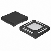
MAX4409ETP+ Maxim Integrated Products, MAX4409ETP+ Datasheet - Page 12

MAX4409ETP+
Manufacturer Part Number
MAX4409ETP+
Description
IC AMP AUDIO .08W STER AB 20TQFN
Manufacturer
Maxim Integrated Products
Series
DirectDrive™r
Type
Class ABr
Datasheet
1.MAX4409ETP.pdf
(20 pages)
Specifications of MAX4409ETP+
Output Type
Headphones, 2-Channel (Stereo)
Max Output Power X Channels @ Load
80mW x 2 @ 16 Ohm
Voltage - Supply
1.8 V ~ 3.6 V
Features
Depop, Short-Circuit and Thermal Protection, Shutdown
Mounting Type
Surface Mount
Package / Case
20-TQFN Exposed Pad
Product
General Purpose Audio Amplifiers
Output Power
80 mW
Common Mode Rejection Ratio (min)
96 dB
Thd Plus Noise
0.002 %
Operating Supply Voltage
1.8 V to 3.6 V
Supply Current
5 mA
Maximum Power Dissipation
2051 mW
Maximum Operating Temperature
+ 85 C
Mounting Style
SMD/SMT
Input Bias Current (max)
0 nA
Input Offset Voltage
0.5 mV
Input Signal Type
Differential
Minimum Operating Temperature
- 40 C
Supply Voltage (max)
3.6 V
Supply Voltage (min)
1.8 V
Amplifier Class
AB
No. Of Channels
2
Supply Voltage Range
1.8V To 3.6V
Load Impedance
16ohm
Operating Temperature Range
-40°C To +85°C
Amplifier Case Style
TQFN
Rohs Compliant
Yes
Lead Free Status / RoHS Status
Lead free / RoHS Compliant
driver. The negative supply voltage appears on the
PV
adjust the contrast of LCD modules.
When considering the use of PV
that the charge-pump voltage at PV
portional to -V
charge-pump output impedance plot appears in the
Typical Operating Characteristics.
External feedback components set the gain of the
MAX4409. Resistors R
Circuit) set the gain of each amplifier as follows:
Choose feedback resistor values of 10kΩ. Values other
than 10kΩ increase V
which in turn increases the amount of DC current flow
to the load. Resistors R
equal value for best results. Use high-tolerance resis-
tors for best matching and CMRR. For example, the
worst-case CMRR attributed to a 1% resistor mismatch
is -34dB. This is the worst case, and typical resistors do
not affect CMRR as drastically. The effect of resistor
mismatch is shown in Figure 5. If all resistors match
exactly, then any voltage applied to node A should be
duplicated on OUT so no net differential voltage
appears between node A (normally the HP jack socket
GND) and OUT. For resistors with a tolerance of n%,
the worst mismatch is found when R
+n%, and R
nominally the same value, then 2n% of the voltage at A
appears between A and OUT.
Packaged resistor arrays can provide well-matched
components for this type of application. Although their
absolute tolerance is not well controlled, the internal
matching of resistors can be very good. At higher fre-
quencies, the rejection is usually limited by PC board
layout; care should be taken to make sure any stray
capacitance due to PC board traces on node N1 match-
es those on node N2. Ultimately, CMRR performance is
limited by the amplifier itself (see Electrical
Characteristics).
The stability of the MAX4409 is affected by the value of
the feedback resistor (R
the input and parasitic trace capacitance introduces an
additional pole. Adding a capacitor in parallel with R
compensates for this pole. Under typical conditions
with proper layout, the device is stable without the
80mW, DirectDrive, Stereo Headphone
Amplifier with Common-Mode Sense
12
SS
______________________________________________________________________________________
pin. A typical application is a negative supply to
F
and R2 are at -n%. If all four resistors are
DD
and is not a regulated voltage. The
A
V
F
= −
OS
and R
IN
F
⎛
⎜
⎝
due to the input bias current,
). The combination of R
, R2, R
R
R
Compensation Capacitor
Component Selection
IN
F
IN
⎞
⎟
⎠
Gain-Setting Resistors
(see Typical Application
SS
F
, and R1 must be of
in this manner, note
SS
IN
is roughly pro-
and R1 are at
F
and
F
additional capacitor.
The input capacitor (C
highpass filter that removes the DC bias from an incom-
ing signal (see Typical Application Circuit). The AC-cou-
pling capacitor allows the amplifier to bias the signal to
an optimum DC level. Assuming zero-source impedance,
the -3dB point of the highpass filter is given by:
Figure 4. Output Power vs. THD+N with Inputs In/Out of Phase
Figure 5. Common-Mode Sense Equivalent Circuit
0.001
0.01
100
0.1
10
1
0
TOTAL HARMONIC DISTORTION PLUS
V
A
R
f
IN
R
R2
DD
V
L
IN
f
= -1V/V
= 16Ω
= 10kHz
-
OUTPUTS IN
PHASE
3
= 3V
dB
NOISE vs. OUTPUT POWER
N1
N2
IN
50
=
OUTPUT POWER (mW)
), in conjunction with R
2
π
R C
MAX4409
IN IN
100
1
R
R1
F
ONE
CHANNEL
150
OUTPUTS
180° OUT OF
PHASE
Input Filtering
OUT
A
200
IN,
forms a


