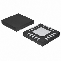
MAX4409ETP+ Maxim Integrated Products, MAX4409ETP+ Datasheet - Page 11

MAX4409ETP+
Manufacturer Part Number
MAX4409ETP+
Description
IC AMP AUDIO .08W STER AB 20TQFN
Manufacturer
Maxim Integrated Products
Series
DirectDrive™r
Type
Class ABr
Datasheet
1.MAX4409ETP.pdf
(20 pages)
Specifications of MAX4409ETP+
Output Type
Headphones, 2-Channel (Stereo)
Max Output Power X Channels @ Load
80mW x 2 @ 16 Ohm
Voltage - Supply
1.8 V ~ 3.6 V
Features
Depop, Short-Circuit and Thermal Protection, Shutdown
Mounting Type
Surface Mount
Package / Case
20-TQFN Exposed Pad
Product
General Purpose Audio Amplifiers
Output Power
80 mW
Common Mode Rejection Ratio (min)
96 dB
Thd Plus Noise
0.002 %
Operating Supply Voltage
1.8 V to 3.6 V
Supply Current
5 mA
Maximum Power Dissipation
2051 mW
Maximum Operating Temperature
+ 85 C
Mounting Style
SMD/SMT
Input Bias Current (max)
0 nA
Input Offset Voltage
0.5 mV
Input Signal Type
Differential
Minimum Operating Temperature
- 40 C
Supply Voltage (max)
3.6 V
Supply Voltage (min)
1.8 V
Amplifier Class
AB
No. Of Channels
2
Supply Voltage Range
1.8V To 3.6V
Load Impedance
16ohm
Operating Temperature Range
-40°C To +85°C
Amplifier Case Style
TQFN
Rohs Compliant
Yes
Lead Free Status / RoHS Status
Lead free / RoHS Compliant
tops, as well as MP3, CD, and DVD players. By elimi-
nating the DC-blocking capacitors through DirectDrive
technology, these capacitor-related deficiencies are
eliminated.
The MAX4409 features a low-noise charge pump. The
320kHz switching frequency is well beyond the audio
range, and thus does not interfere with the audio sig-
nals. The switch drivers feature a controlled switching
speed that minimizes noise generated by turn-on and
turn-off transients. By limiting the switching speed of the
switches, the di/dt noise caused by the parasitic bond
wire and trace inductance is minimized. Although not
typically required, additional high-frequency noise atten-
uation can be achieved by increasing the size of C2
(see Typical Application Circuit).
The MAX4409 features an active-low SHDN control.
Driving SHDN low disables the charge pump and
amplifiers, sets the amplifier output impedance to
approximately 1kΩ, and reduces supply current draw
to less than 6µA.
In traditional single-supply audio drivers, the output-
coupling capacitor is a major contributor of audible
clicks and pops. Upon startup, the driver charges the
coupling capacitor to its bias voltage, typically half the
supply. Likewise, on shutdown the capacitor is dis-
charged to GND. This results in a DC shift across the
capacitor, which in turn, appears as an audible transient
at the speaker. Since the MAX4409 does not require
output-coupling capacitors, this does not arise.
Additionally, the MAX4409 features extensive click-and-
pop suppression that eliminates any audible transient
sources internal to the device. The Power-Up/Down
Waveform in the Typical Operating Characteristics
shows that there are minimal spectral components in the
audible range at the output upon startup or shutdown.
In most applications, the output of the preamplifier dri-
ving the MAX4409 has a DC bias of typically half the
supply. At startup, the input-coupling capacitor is
charged to the preamplifier’s DC-bias voltage through
the R
the capacitor and an audible click/pop. Delaying the
rise of the SHDN_ signals 4 to 5 time constants (40ms
to 50ms) based on R
the preamplifier eliminates this click/pop caused by the
input filter.
F
of the MAX4409, resulting in a DC shift across
______________________________________________________________________________________
Click-and-Pop Suppression
IN
80mW, DirectDrive, Stereo Headphone
and C
Amplifier with Common-Mode Sense
IN
relative to the start of
Charge Pump
Shutdown
Under normal operating conditions, linear power ampli-
fiers can dissipate a significant amount of power. The
maximum power dissipation for each package is given
in the Absolute Maximum Ratings section under
Continuous Power Dissipation or can be calculated by
the following equation:
where T
and θ
specified in the Absolute Maximum Ratings section. For
example, θ
The MAX4409 has two sources of power dissipation,
the charge pump and two drivers. If the power dissipa-
tion for a given application exceeds the maximum
allowed for a given package, either reduce V
increase load impedance, decrease the ambient tem-
perature, or add heat sinking to the device. Large out-
put, supply, and ground traces improve the maximum
power dissipation in the package.
Thermal overload protection limits total power dissipa-
tion in the MAX4409. When the junction temperature
exceeds +140°C, the thermal-protection circuitry dis-
ables the amplifier output stage. The amplifiers are
enabled once the junction temperature cools by 15°C.
This results in a pulsing output under continuous ther-
mal-overload conditions.
The device has been specified for the worst-case sce-
nario—when both inputs are in phase. Under this con-
dition, the drivers simultaneously draw current from the
charge pump, leading to a slight loss in headroom of
V
right signals have differences in both magnitude and
phase, subsequently leading to an increase in the max-
imum attainable output power. Figure 4 shows the two
extreme cases for in and out of phase. In reality, the
available power lies between these extremes.
An additional benefit of the MAX4409 is the internally
generated, negative supply voltage (PV
age is used by the MAX4409 to provide the ground-ref-
erenced output level. It can, however, also be used to
power other devices within a design. Current draw from
this negative supply (PV
exceeding this affects the operation of the headphone
SS
. In typical stereo audio applications, the left and
JA
J(MAX)
is the reciprocal of the derating factor in °C/W as
JA
P
DISSPKG MAX
of the TQFN package is +39°C/W.
is +150°C, T
Powering Other Circuits from a
Applications Information
(
SS
)
=
A
) should be limited to 5mA;
T
is the ambient temperature,
J MAX
(
Power Dissipation
θ
JA
Negative Supply
)
−
T
A
Output Power
SS
). This volt-
DD
11
,


