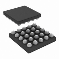
LM4846TL/NOPB National Semiconductor, LM4846TL/NOPB Datasheet - Page 21

LM4846TL/NOPB
Manufacturer Part Number
LM4846TL/NOPB
Description
IC AMP AUDIO PWR 1.15W AB 25USMD
Manufacturer
National Semiconductor
Series
Boomer®r
Type
Class ABr
Datasheet
1.LM4846TLNOPB.pdf
(30 pages)
Specifications of LM4846TL/NOPB
Output Type
1-Channel (Mono) with Stereo Headphones
Max Output Power X Channels @ Load
1.15W x 1 @ 8 Ohm; 75mW x 2 @ 32 Ohm
Voltage - Supply
2.7 V ~ 5.5 V
Features
3D, Depop, I²C, Mute, Shutdown, SPI, Thermal Protection, Volume Control
Mounting Type
Surface Mount
Package / Case
25-MicroSMD
Operational Class
Class-AB
Audio Amplifier Function
Headphone/Speaker
Total Harmonic Distortion
0.5@8Ohm@500mW%
Single Supply Voltage (typ)
3/5V
Dual Supply Voltage (typ)
Not RequiredV
Supply Current (max)
11@3.3VmA
Power Supply Requirement
Single
Rail/rail I/o Type
No
Power Supply Rejection Ratio
88dB
Single Supply Voltage (min)
2.7V
Single Supply Voltage (max)
5.5V
Dual Supply Voltage (min)
Not RequiredV
Dual Supply Voltage (max)
Not RequiredV
Operating Temp Range
-40C to 85C
Operating Temperature Classification
Industrial
Mounting
Surface Mount
Pin Count
25
Package Type
uSMD
For Use With
LM4846TLEVAL - BOARD EVALUATION LM4846TL
Lead Free Status / RoHS Status
Lead free / RoHS Compliant
Other names
LM4846TLTR
Application Information
SPI DESCRIPTION
0. I
1. The data bits are transmitted with the MSB first.
2. The maximum clock rate is 1MHz for the CLK pin.
3. CLK must remain HIGH for at least 500ns (t
rising edge of CLK, and CLK must remain LOW for at least
500ns (t
4. The serial data bits are sampled at the rising edge of CLK.
Any transition on DATA must occur at least 100ns (t
before the rising edge of CLK. Also, any transition on DATA
must occur at least 100ns (t
and stabilize before the next rising edge of CLK.
5.ID_ENB should be LOW only during serial data transmis-
sion.
6. ID_ENB must be LOW at least 100ns (t
rising edge of CLK, and ID_ENB has to remain LOW at least
100ns (t
2
CSPI_SEL: This pin is tied HIGH for SPI mode.
CL
EH
) after the falling edge of CLK.
) after the eighth rising edge of CLK.
DH
) after the rising edge of CLK
ES
(Continued)
) before the first
CH
FIGURE 5. SPI Timing Diagram
FIGURE 4. I
) after the
DS
)
2
C Timing Diagram
21
7. If ID_ENB remains HIGH for more than 100ns before all 8
bits are transmitted then the data latch will be aborted.
8. If ID_ENB is LOW for more than 8 CLK pulses then only
the first 8 data bits will be latched and activated when
ID_ENB transitions to logic-high.
9. ID_ENB must remain HIGH for at least 100ns (t
in the data.
10. Coincidental rising or falling edges of CLK and ID_ENB
are not allowed. If CLK is to be held HIGH after the data
transmission, the falling edge of CLK must occur at least
100ns (t
set of data.
CS
) before ID_ENB transitions to LOW for the next
20166824
201668F4
www.national.com
EL
) to latch


