LM4846TL/NOPB National Semiconductor, LM4846TL/NOPB Datasheet - Page 20
LM4846TL/NOPB
Manufacturer Part Number
LM4846TL/NOPB
Description
IC AMP AUDIO PWR 1.15W AB 25USMD
Manufacturer
National Semiconductor
Series
Boomer®r
Type
Class ABr
Datasheet
1.LM4846TLNOPB.pdf
(30 pages)
Specifications of LM4846TL/NOPB
Output Type
1-Channel (Mono) with Stereo Headphones
Max Output Power X Channels @ Load
1.15W x 1 @ 8 Ohm; 75mW x 2 @ 32 Ohm
Voltage - Supply
2.7 V ~ 5.5 V
Features
3D, Depop, I²C, Mute, Shutdown, SPI, Thermal Protection, Volume Control
Mounting Type
Surface Mount
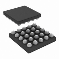
Package / Case
25-MicroSMD
Operational Class
Class-AB
Audio Amplifier Function
Headphone/Speaker
Total Harmonic Distortion
0.5@8Ohm@500mW%
Single Supply Voltage (typ)
3/5V
Dual Supply Voltage (typ)
Not RequiredV
Supply Current (max)
11@3.3VmA
Power Supply Requirement
Single
Rail/rail I/o Type
No
Power Supply Rejection Ratio
88dB
Single Supply Voltage (min)
2.7V
Single Supply Voltage (max)
5.5V
Dual Supply Voltage (min)
Not RequiredV
Dual Supply Voltage (max)
Not RequiredV
Operating Temp Range
-40C to 85C
Operating Temperature Classification
Industrial
Mounting
Surface Mount
Pin Count
25
Package Type
uSMD
For Use With
LM4846TLEVAL - BOARD EVALUATION LM4846TL
Lead Free Status / RoHS Status
Lead free / RoHS Compliant
Other names
LM4846TLTR


www.national.com
Application Information
I
SDA: This is the serial data input pin.
SCL: This is the clock input pin.
ID_ENB: This is the address select input pin.
I
I
The LM4846 uses a serial bus which conforms to the I
protocol to control the chip’s functions with two wires: clock
(SCL) and data (SDA). The clock line is uni-directional. The
data line is bi-directional (open-collector). The maximum
clock frequency specified by the I
this discussion, the master is the controlling microcontroller
and the slave is the LM4846.
The I
ID_ENB pin. The LM4846’s two possible I
are of the form 111110X
is logic LOW; and X
interface is used to address a number of chips in a system,
the LM4846’s chip address can be changed to avoid any
possible address conflicts.
The bus format for the I
bus format diagram is broken up into six major sections:
The "start" signal is generated by lowering the data signal
while the clock signal is HIGH. The start signal will alert all
devices attached to the I
dress against their own address.
The 8-bit chip address is sent next, most significant bit first.
The data is latched in on the rising edge of the clock. Each
address bit must be stable while the clock level is HIGH.
2
2
2
C PIN DESCRIPTION
CSPI_SEL: This is tied LOW for I
C COMPATIBLE INTERFACE
2
C address for the LM4846 is determined using the
1
= 1, if ID_ENB is logic HIGH. If the I
2
1
C interface is shown in Figure 3. The
0 (binary), where X
2
C bus to check the incoming ad-
2
C standard is 400kHz. In
2
C mode.
2
C chip addresses
1
= 0, if ID_ENB
FIGURE 3. I
2
2
C
C
2
20
C Bus Format
For I
tied LOW (and tied high for SPI operation).
After the last bit of the address bit is sent, the master
releases the data line HIGH (through a pull-up resistor).
Then the master sends an acknowledge clock pulse. If the
LM4846 has received the address correctly, then it holds the
data line LOW during the clock pulse. If the data line is not
held LOW during the acknowledge clock pulse, then the
master should abort the rest of the data transfer to the
LM4846.
The 8 bits of data are sent next, most significant bit first.
Each data bit should be valid while the clock level is stable
HIGH.
After the data byte is sent, the master must check for another
acknowledge to see if the LM4846 received the data.
If the master has more data bytes to send to the LM4846,
then the master can repeat the previous two steps until all
data bytes have been sent.
The "stop" signal ends the transfer. To signal "stop", the data
signal goes HIGH while the clock signal is HIGH. The data
line should be held HIGH when not in use.
I
The LM4846’s I
I
age level set by the I
dent to that of the main power supply pin V
whenever logic levels for the I
microcontroller or microprocessor that is operating at a lower
supply voltage than the main battery of a portable system.
2
2
C INTERFACE POWER SUPPLY PIN (I
CV
2
DD
C interface operation, the I
pin. The LM4846’s I
2
C interface is powered up through the
2
CV
DD
2
pin which can be set indepen-
C interface operates at a volt-
2
C interface are dictated by a
2
CSPI_SEL pin needs to be
2
CV
DD
DD
. This is ideal
201668F5
)
Related parts for LM4846TL/NOPB
Image
Part Number
Description
Manufacturer
Datasheet
Request
R

Part Number:
Description:
National Semiconductor [8-Bit D/A Converter]
Manufacturer:
National Semiconductor
Datasheet:
Part Number:
Description:
National Semiconductor [Media Coprocessor]
Manufacturer:
National Semiconductor
Datasheet:
Part Number:
Description:
Digitally Controlled Tone and Volume Circuit with Stereo Audio Power Amplifier, Microphone Preamp Stage and National 3D Sound
Manufacturer:
National Semiconductor
Datasheet:
Part Number:
Description:
Digitally Controlled Tone and Volume Circuit with Stereo Audio Power Amplifier, Microphone Preamp Stage and National 3D Sound
Manufacturer:
National Semiconductor
Datasheet:
Part Number:
Description:
AC97 Rev 2 Codec with Sample Rate Conversion and National 3D Sound
Manufacturer:
National Semiconductor
Part Number:
Description:
Manufacturer:
National Semiconductor
Datasheet:
Part Number:
Description:
Manufacturer:
National Semiconductor
Datasheet:
Part Number:
Description:
General Purpose, Low Voltage, Low Power, Rail-to-Rail Output Operational Amplifiers
Manufacturer:
National Semiconductor
Datasheet:
Part Number:
Description:
8-bit 20 MSPS flash A/D converter.
Manufacturer:
National Semiconductor
Datasheet:
Part Number:
Description:
Low Noise Quad Operational Amplifier
Manufacturer:
National Semiconductor
Datasheet:
Part Number:
Description:
Quad Differential Line Receivers
Manufacturer:
National Semiconductor
Datasheet:
Part Number:
Description:
Quad High Speed Trapezoidal? Bus Transceiver
Manufacturer:
National Semiconductor
Datasheet:
Part Number:
Description:
Dual Line Receiver
Manufacturer:
National Semiconductor
Datasheet:
Part Number:
Description:
TTL to 10k ECL Level Translator with Latch
Manufacturer:
National Semiconductor
Datasheet: