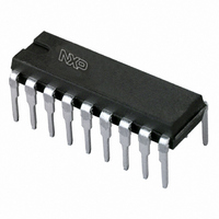
TDA1517P/N3,112 NXP Semiconductors, TDA1517P/N3,112 Datasheet - Page 4

TDA1517P/N3,112
Manufacturer Part Number
TDA1517P/N3,112
Description
IC AMP AUDIO PWR 6W STER 18HDIP
Manufacturer
NXP Semiconductors
Type
Class Br
Datasheet
1.TDA1517N3112.pdf
(15 pages)
Specifications of TDA1517P/N3,112
Output Type
2-Channel (Stereo)
Package / Case
18-DIP (0.300", 7.62mm) Exposed Pad
Max Output Power X Channels @ Load
6W x 2 @ 4 Ohm
Voltage - Supply
6 V ~ 18 V
Features
Depop, Mute, Short-Circuit and Thermal Protection, Standby
Mounting Type
Through Hole
Product
Class-B
Output Power
6 W
Available Set Gain
20 dB
Thd Plus Noise
0.1 %
Operating Supply Voltage
14.4 V
Supply Current
40 mA
Maximum Power Dissipation
15000 mW
Maximum Operating Temperature
+ 85 C
Mounting Style
Through Hole
Audio Load Resistance
4 Ohms
Input Signal Type
Single
Minimum Operating Temperature
- 40 C
Output Signal Type
Single
Supply Type
Single
Supply Voltage (max)
18 V
Supply Voltage (min)
6 V
Operational Class
Class-B
Audio Amplifier Output Configuration
2-Channel Stereo
Output Power (typ)
6x2@4OhmW
Audio Amplifier Function
Speaker
Total Harmonic Distortion
0.1@4Ohm@1W%
Single Supply Voltage (typ)
14.4V
Dual Supply Voltage (typ)
Not RequiredV
Power Supply Requirement
Single
Power Dissipation
15W
Rail/rail I/o Type
No
Power Supply Rejection Ratio
80dB
Single Supply Voltage (min)
6V
Single Supply Voltage (max)
18V
Dual Supply Voltage (min)
Not RequiredV
Dual Supply Voltage (max)
Not RequiredV
Operating Temp Range
-40C to 85C
Operating Temperature Classification
Industrial
Mounting
Through Hole
Pin Count
18
Lead Free Status / RoHS Status
Lead free / RoHS Compliant
Lead Free Status / RoHS Status
Lead free / RoHS Compliant, Lead free / RoHS Compliant
Other names
568-1128-5
935261850112
TDA1517PN
935261850112
TDA1517PN
NXP Semiconductors
PINNING
FUNCTIONAL DESCRIPTION
The TDA1517 contains two identical amplifiers with
differential input stages. The gain of each amplifier is fixed
at 20 dB. A special feature of the device is the
mute/standby switch which has the following features:
• Low standby current (<100 μA)
• Low mute/standby switching current
• Mute condition.
2004 Feb 18
handbook, halfpage
−INV1
SGND
SVRR
OUT1
PGND
OUT2
V
M/SS
−INV2
(low cost supply switch)
P
2 x 6 W stereo power amplifier
Fig.2
SYMBOL
Pin configuration for SOT110-1 and
SOT352-1.
SGND
PGND
SVRR
OUT1
OUT2
M/SS
INV1
INV2
V
P
3
4
1
2
5
6
7
8
9
TDA1517
MLC352
PIN
1
2
3
4
5
6
7
8
9
non-inverting input 1
signal ground
supply voltage ripple rejection output
output 1
power ground
output 2
supply voltage
mute/standby switch input
non-inverting input 2
4
handbook, halfpage
Pins 10 to 18 should be connected to GND or floating.
Fig.3 Pin configuration for SOT398-1.
DESCRIPTION
SGND
PGND
SVRR
OUT1
OUT2
M/SS
INV1
INV2
V
P
TDA1517; TDA1517P
3
4
1
2
5
6
7
8
9
TDA1517P
MLC353
Product specification
16
15
18
17
14
13
12
11
10


