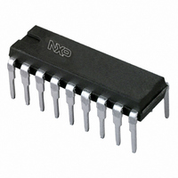
TDA1517P/N3,112 NXP Semiconductors, TDA1517P/N3,112 Datasheet - Page 12

TDA1517P/N3,112
Manufacturer Part Number
TDA1517P/N3,112
Description
IC AMP AUDIO PWR 6W STER 18HDIP
Manufacturer
NXP Semiconductors
Type
Class Br
Datasheet
1.TDA1517N3112.pdf
(15 pages)
Specifications of TDA1517P/N3,112
Output Type
2-Channel (Stereo)
Package / Case
18-DIP (0.300", 7.62mm) Exposed Pad
Max Output Power X Channels @ Load
6W x 2 @ 4 Ohm
Voltage - Supply
6 V ~ 18 V
Features
Depop, Mute, Short-Circuit and Thermal Protection, Standby
Mounting Type
Through Hole
Product
Class-B
Output Power
6 W
Available Set Gain
20 dB
Thd Plus Noise
0.1 %
Operating Supply Voltage
14.4 V
Supply Current
40 mA
Maximum Power Dissipation
15000 mW
Maximum Operating Temperature
+ 85 C
Mounting Style
Through Hole
Audio Load Resistance
4 Ohms
Input Signal Type
Single
Minimum Operating Temperature
- 40 C
Output Signal Type
Single
Supply Type
Single
Supply Voltage (max)
18 V
Supply Voltage (min)
6 V
Operational Class
Class-B
Audio Amplifier Output Configuration
2-Channel Stereo
Output Power (typ)
6x2@4OhmW
Audio Amplifier Function
Speaker
Total Harmonic Distortion
0.1@4Ohm@1W%
Single Supply Voltage (typ)
14.4V
Dual Supply Voltage (typ)
Not RequiredV
Power Supply Requirement
Single
Power Dissipation
15W
Rail/rail I/o Type
No
Power Supply Rejection Ratio
80dB
Single Supply Voltage (min)
6V
Single Supply Voltage (max)
18V
Dual Supply Voltage (min)
Not RequiredV
Dual Supply Voltage (max)
Not RequiredV
Operating Temp Range
-40C to 85C
Operating Temperature Classification
Industrial
Mounting
Through Hole
Pin Count
18
Lead Free Status / RoHS Status
Lead free / RoHS Compliant
Lead Free Status / RoHS Status
Lead free / RoHS Compliant, Lead free / RoHS Compliant
Other names
568-1128-5
935261850112
TDA1517PN
935261850112
TDA1517PN
NXP Semiconductors
SOLDERING
Introduction to soldering through-hole mount
packages
This text gives a brief insight to wave, dip and manual
soldering. A more in-depth account of soldering ICs can be
found in our “Data Handbook IC26; Integrated Circuit
Packages” (document order number 9398 652 90011).
Wave soldering is the preferred method for mounting of
through-hole mount IC packages on a printed-circuit
board.
Soldering by dipping or by solder wave
Driven by legislation and environmental forces the
worldwide use of lead-free solder pastes is increasing.
Typical dwell time of the leads in the wave ranges from
3 to 4 seconds at 250 °C or 265 °C, depending on solder
material applied, SnPb or Pb-free respectively.
Suitability of through-hole mount IC packages for dipping and wave soldering methods
Notes
1. For SDIP packages, the longitudinal axis must be parallel to the transport direction of the printed-circuit board.
2. For PMFP packages hot bar soldering or manual soldering is suitable.
2004 Feb 18
CPGA, HCPGA
DBS, DIP, HDIP, RDBS, SDIP, SIL
PMFP
2 x 6 W stereo power amplifier
(2)
PACKAGE
−
suitable
−
DIPPING
12
The total contact time of successive solder waves must not
exceed 5 seconds.
The device may be mounted up to the seating plane, but
the temperature of the plastic body must not exceed the
specified maximum storage temperature (T
printed-circuit board has been pre-heated, forced cooling
may be necessary immediately after soldering to keep the
temperature within the permissible limit.
Manual soldering
Apply the soldering iron (24 V or less) to the lead(s) of the
package, either below the seating plane or not more than
2 mm above it. If the temperature of the soldering iron bit
is less than 300 °C it may remain in contact for up to
10 seconds. If the bit temperature is between
300 and 400 °C, contact may be up to 5 seconds.
SOLDERING METHOD
suitable
suitable
not suitable
TDA1517; TDA1517P
(1)
WAVE
Product specification
stg(max)
). If the


