SA58670ABS,115 NXP Semiconductors, SA58670ABS,115 Datasheet - Page 21
SA58670ABS,115
Manufacturer Part Number
SA58670ABS,115
Description
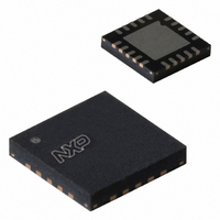
IC AMP AUDIO 2.1W STER D 20HVQFN
Manufacturer
NXP Semiconductors
Type
Class Dr
Specifications of SA58670ABS,115
Output Type
2-Channel (Stereo)
Package / Case
20-VQFN Exposed Pad, 20-HVQFN, 20-SQFN, 20-DHVQFN
Max Output Power X Channels @ Load
2.1W x 2 @ 4 Ohm
Voltage - Supply
2.5 V ~ 5.5 V
Features
Differential Inputs, Short-Circuit and Thermal Protection, Shutdown
Mounting Type
Surface Mount
Product
Class-D
Output Power
2.1 W
Available Set Gain
24 dB
Common Mode Rejection Ratio (min)
69 dB
Thd Plus Noise
0.14 %, 0.11 %
Operating Supply Voltage
3 V, 5 V
Supply Current
6 mA
Maximum Power Dissipation
5.2 W
Maximum Operating Temperature
+ 85 C
Mounting Style
SMD/SMT
Audio Load Resistance
8 Ohms
Input Signal Type
Differential
Minimum Operating Temperature
- 40 C
Output Signal Type
Differential
Supply Type
Single
Supply Voltage (max)
5.5 V
Supply Voltage (min)
2.5 V
Lead Free Status / RoHS Status
Lead free / RoHS Compliant
Lead Free Status / RoHS Status
Lead free / RoHS Compliant, Lead free / RoHS Compliant
Other names
568-4354-2
935286181115
SA58670ABS
SA58670ABS-G
SA58670ABS-G
935286181115
SA58670ABS
SA58670ABS-G
SA58670ABS-G


NXP Semiconductors
SA58670_3
Product data sheet
13.4 Reflow soldering
Key characteristics in reflow soldering are:
Table 7.
Table 8.
Moisture sensitivity precautions, as indicated on the packing, must be respected at all
times.
Studies have shown that small packages reach higher temperatures during reflow
soldering, see
Package thickness (mm)
< 2.5
Package thickness (mm)
< 1.6
1.6 to 2.5
> 2.5
•
•
•
2.5
Lead-free versus SnPb soldering; note that a lead-free reflow process usually leads to
higher minimum peak temperatures (see
reducing the process window
Solder paste printing issues including smearing, release, and adjusting the process
window for a mix of large and small components on one board
Reflow temperature profile; this profile includes preheat, reflow (in which the board is
heated to the peak temperature) and cooling down. It is imperative that the peak
temperature is high enough for the solder to make reliable solder joints (a solder paste
characteristic). In addition, the peak temperature must be low enough that the
packages and/or boards are not damaged. The peak temperature of the package
depends on package thickness and volume and is classified in accordance with
Table 7
SnPb eutectic process (from J-STD-020C)
Lead-free process (from J-STD-020C)
and
Figure
8
18.
Rev. 03 — 11 June 2009
Package reflow temperature ( C)
Volume (mm
< 350
235
220
Package reflow temperature ( C)
Volume (mm
< 350
260
260
250
3
3
)
)
2.1 W/channel stereo class-D audio amplifier
Figure
350 to 2000
260
250
245
18) than a SnPb process, thus
220
220
350
> 2000
260
245
245
SA58670
© NXP B.V. 2009. All rights reserved.
21 of 25
Related parts for SA58670ABS,115
Image
Part Number
Description
Manufacturer
Datasheet
Request
R

Part Number:
Description:
Manufacturer:
NXP Semiconductors
Datasheet:

Part Number:
Description:
NXP Semiconductors designed the LPC2420/2460 microcontroller around a 16-bit/32-bitARM7TDMI-S CPU core with real-time debug interfaces that include both JTAG andembedded trace
Manufacturer:
NXP Semiconductors
Datasheet:

Part Number:
Description:
NXP Semiconductors designed the LPC2458 microcontroller around a 16-bit/32-bitARM7TDMI-S CPU core with real-time debug interfaces that include both JTAG andembedded trace
Manufacturer:
NXP Semiconductors
Datasheet:
Part Number:
Description:
NXP Semiconductors designed the LPC2468 microcontroller around a 16-bit/32-bitARM7TDMI-S CPU core with real-time debug interfaces that include both JTAG andembedded trace
Manufacturer:
NXP Semiconductors
Datasheet:
Part Number:
Description:
NXP Semiconductors designed the LPC2470 microcontroller, powered by theARM7TDMI-S core, to be a highly integrated microcontroller for a wide range ofapplications that require advanced communications and high quality graphic displays
Manufacturer:
NXP Semiconductors
Datasheet:
Part Number:
Description:
NXP Semiconductors designed the LPC2478 microcontroller, powered by theARM7TDMI-S core, to be a highly integrated microcontroller for a wide range ofapplications that require advanced communications and high quality graphic displays
Manufacturer:
NXP Semiconductors
Datasheet:
Part Number:
Description:
The Philips Semiconductors XA (eXtended Architecture) family of 16-bit single-chip microcontrollers is powerful enough to easily handle the requirements of high performance embedded applications, yet inexpensive enough to compete in the market for hi
Manufacturer:
NXP Semiconductors
Datasheet:
Part Number:
Description:
The XA-S3 device is a member of Philips Semiconductors? XA(eXtended Architecture) family of high performance 16-bitsingle-chip microcontrollers
Manufacturer:
NXP Semiconductors
Datasheet:

Part Number:
Description:
The NXP BlueStreak LH75401/LH75411 family consists of two low-cost 16/32-bit System-on-Chip (SoC) devices
Manufacturer:
NXP Semiconductors
Datasheet:
Part Number:
Description:
The NXP LPC3130/3131 combine an 180 MHz ARM926EJ-S CPU core, high-speed USB2
Manufacturer:
NXP Semiconductors
Datasheet:
Part Number:
Description:
The NXP LPC3141 combine a 270 MHz ARM926EJ-S CPU core, High-speed USB 2
Manufacturer:
NXP Semiconductors
Part Number:
Description:
The NXP LPC3143 combine a 270 MHz ARM926EJ-S CPU core, High-speed USB 2
Manufacturer:
NXP Semiconductors

Part Number:
Description:
The NXP LPC3152 combines an 180 MHz ARM926EJ-S CPU core, High-speed USB 2
Manufacturer:
NXP Semiconductors
Part Number:
Description:
The NXP LPC3154 combines an 180 MHz ARM926EJ-S CPU core, High-speed USB 2
Manufacturer:
NXP Semiconductors