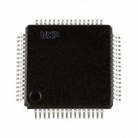
SC16C554IB64,151 NXP Semiconductors, SC16C554IB64,151 Datasheet - Page 25

SC16C554IB64,151
Manufacturer Part Number
SC16C554IB64,151
Description
IC UART QUAD SOT314-2
Manufacturer
NXP Semiconductors
Specifications of SC16C554IB64,151
Number Of Channels
4, QUART
Fifo's
16 Byte
Voltage - Supply
2.5V, 3.3V, 5V
With Auto Flow Control
Yes
With Irda Encoder/decoder
Yes
With False Start Bit Detection
Yes
With Modem Control
Yes
With Cmos
Yes
Mounting Type
Surface Mount
Package / Case
64-LQFP
Transmit Fifo
16Byte
Receive Fifo
16Byte
Transmitter And Receiver Fifo Counter
Yes
Data Rate
5Mbps
Package Type
LQFP
Operating Supply Voltage (max)
5.5V
Operating Supply Voltage (min)
4.5V
Mounting
Surface Mount
Operating Temperature (min)
-40C
Operating Temperature (max)
85C
Operating Temperature Classification
Industrial
Lead Free Status / RoHS Status
Lead free / RoHS Compliant
Other names
935270074151
SC16C554IB64-S
SC16C554IB64-S
SC16C554IB64-S
SC16C554IB64-S
Philips Semiconductors
9397 750 11616
Product data
Table 10:
Table 11:
Bit
2
1
0
FCR[7]
0
0
1
1
Symbol
FCR[2]
FCR[1]
FCR[0]
FIFO Control Register bits description
RCVR trigger levels
Quad UART with 16-byte FIFO and infrared (IrDA) encoder/decoder
FCR[6]
0
1
0
1
Rev. 04 — 19 June 2003
Description
Transmit operation in mode ‘1’: When the SC16C554/554D is in FIFO
mode (FCR[0] = logic 1; FCR[3] = logic 1), the TXRDY pin will be a
logic 1 when the transmit FIFO is completely full. It will be a logic 0 if one
or more FIFO locations are empty.
Receive operation in mode ‘1’: When the SC16C554/554D is in FIFO
mode (FCR[0] = logic 1; FCR[3] = logic 1) and the trigger level has been
reached, or a Receive Time-Out has occurred, the RXRDY pin will go to
a logic 0. Once activated, it will go to a logic 1 after there are no more
characters in the FIFO.
XMIT FIFO reset.
RCVR FIFO reset.
FIFO enable.
Logic 0 = No FIFO transmit reset (normal default condition).
Logic 1 = Clears the contents of the transmit FIFO and resets the
FIFO counter logic (the transmit shift register is not cleared or
altered). This bit will return to a logic 0 after clearing the FIFO.
Logic 0 = No FIFO receive reset (normal default condition).
Logic 1 = Clears the contents of the receive FIFO and resets the FIFO
counter logic (the receive shift register is not cleared or altered). This
bit will return to a logic 0 after clearing the FIFO.
Logic 0 = Disable the transmit and receive FIFO (normal default
condition).
Logic 1 = Enable the transmit and receive FIFO. This bit must be a
‘1’ when other FCR bits are written to, or they will not be
programmed.
RX FIFO trigger level
1
4
8
14
…continued
SC16C554/554D
© Koninklijke Philips Electronics N.V. 2003. All rights reserved.
25 of 53


