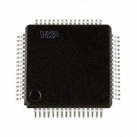
SC16C554IB64,151 NXP Semiconductors, SC16C554IB64,151 Datasheet - Page 12

SC16C554IB64,151
Manufacturer Part Number
SC16C554IB64,151
Description
IC UART QUAD SOT314-2
Manufacturer
NXP Semiconductors
Specifications of SC16C554IB64,151
Number Of Channels
4, QUART
Fifo's
16 Byte
Voltage - Supply
2.5V, 3.3V, 5V
With Auto Flow Control
Yes
With Irda Encoder/decoder
Yes
With False Start Bit Detection
Yes
With Modem Control
Yes
With Cmos
Yes
Mounting Type
Surface Mount
Package / Case
64-LQFP
Transmit Fifo
16Byte
Receive Fifo
16Byte
Transmitter And Receiver Fifo Counter
Yes
Data Rate
5Mbps
Package Type
LQFP
Operating Supply Voltage (max)
5.5V
Operating Supply Voltage (min)
4.5V
Mounting
Surface Mount
Operating Temperature (min)
-40C
Operating Temperature (max)
85C
Operating Temperature Classification
Industrial
Lead Free Status / RoHS Status
Lead free / RoHS Compliant
Other names
935270074151
SC16C554IB64-S
SC16C554IB64-S
SC16C554IB64-S
SC16C554IB64-S
Philips Semiconductors
Table 2:
9397 750 11616
Product data
Symbol
RXA, RXB,
RXC, RXD
RXRDY
TXA, TXB,
TXC, TXD
TXRDY
V
XTAL1
XTAL2
CC
Pin description
Pin
PLCC68 LQFP64 LQFP80
7, 29,
41, 63
38
17, 19,
51, 53
39
13, 30,
47, 64
35
36
62, 20,
29, 51
-
8, 10,
39, 41
-
4, 21,
35, 52
25
26
…continued
17, 44,
57, 4
54
29, 32,
69, 72
55
5, 25,
45, 65
50
51
Quad UART with 16-byte FIFO and infrared (IrDA) encoder/decoder
Type
I
O
O
O
I
I
O
Rev. 04 — 19 June 2003
Description
Receive data input RXA-RXD. These inputs are associated with
individual serial channel data to the SC16C554/554D. The RX signal
will be a logic 1 during reset, idle (no data), or when the transmitter is
disabled. During the local loop-back mode, the RX input pin is
disabled and TX data is connected to the UART RX input internally.
Receive Ready (Active-LOW). This function is associated with
68-pin package only. RXRDY contains the wire-ORed status of all
four receive channel FIFOs, RXRDYA-RXRDYD. A logic 0 indicates
receive data ready status, i.e., the RHR is full, or the FIFO has one or
more RX characters available for unloading. This pin goes to a
logic 1 when the FIFO/RHR is empty, or when there are no more
characters available in either the FIFO or RHR. Individual channel
RX status is read by examining individual internal registers via CS
and A0-A4 pin functions.
Transmit data A, B, C, D. These outputs are associated with
individual serial transmit channel data from the SC16C554/554D.
The TX signal will be a logic 1 during reset, idle (no data), or when
the transmitter is disabled. During the local loop-back mode, the TX
output pin is disabled and TX data is internally connected to the
UART RX input.
Transmit Ready (Active-LOW). This function is associated with the
68-pin package only. TXRDY contains the wire-ORed status of all
four transmit channel FIFOs, TXRDYA-TXRDYD. A logic 0 indicates a
buffer ready status, i.e., at least one location is empty and available in
one of the TX channels (A-D). This pin goes to a logic 1 when all four
channels have no more empty locations in the TX FIFO or THR.
Individual channel TX status can be read by examining individual
internal registers via CS and A0-A4 pin functions.
Power supply inputs.
Crystal or external clock input. Functions as a crystal input or as
an external clock input. A crystal can be connected between this pin
and XTAL2 to form an internal oscillator circuit (see
Alternatively, an external clock can be connected to this pin to
provide custom data rates. (See
rate
Output of the crystal oscillator or buffered clock. (See also
XTAL1.) Crystal oscillator output or buffered clock output.
generator”.)
SC16C554/554D
Section 6.10 “Programmable baud
© Koninklijke Philips Electronics N.V. 2003. All rights reserved.
Figure
7).
12 of 53


