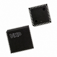
SCC2681TC1A44,518 NXP Semiconductors, SCC2681TC1A44,518 Datasheet - Page 5

SCC2681TC1A44,518
Manufacturer Part Number
SCC2681TC1A44,518
Description
IC DUART SOT187-2
Manufacturer
NXP Semiconductors
Datasheet
1.SCC2681TC1A44518.pdf
(15 pages)
Specifications of SCC2681TC1A44,518
Features
False-start Bit Detection
Number Of Channels
2, DUART
Fifo's
3Bit
Voltage - Supply
4.5 V ~ 5.5 V
With Parallel Port
Yes
With Auto Flow Control
Yes
With False Start Bit Detection
Yes
With Cmos
Yes
Mounting Type
Surface Mount
Package / Case
44-LCC (J-Lead)
Lead Free Status / RoHS Status
Lead free / RoHS Compliant
Other names
935274519518
SCC2681TC1A44-T
SCC2681TC1A44-T
SCC2681TC1A44-T
SCC2681TC1A44-T
Philips Semiconductors
2004 Apr 06
MNEMONIC
Dual asynchronous receiver/transmitter (DUART)
TxDA
TxDB
GND
OP0
OP1
OP2
OP3
OP4
OP5
OP6
OP7
V
n.c.
IP0
IP1
IP2
IP3
IP4
IP5
IP6
CC
1, 12, 23,
PIN
33
13
32
14
31
15
30
16
29
17
40
43
42
41
44
22
34
8
5
3
TYPE
O
O
O
O
O
O
O
O
O
O
I
I
I
I
I
I
I
I
I
Channel A Transmitter Serial Data Output: The least significant bit is transmitted first. This output is held
in the ‘mark’ condition when the transmitter is disabled, idle, or when operating in local loopback mode.
‘Mark’ is HIGH, ‘space’ is LOW.
Channel B Transmitter Serial Data Output: The least significant bit is transmitted first. This output is
held in the ‘mark’ condition when the transmitter is disabled, idle, or when operating in local loopback
mode. ‘Mark’ is HIGH, ‘space’ is LOW.
Output 0: General purpose output, or channel A request to send (RTSAN, active-LOW). Can be
deactivated automatically on receive or transmit.
Output 1: General purpose output, or channel B request to send (RTSBN, active-LOW). Can be
deactivated automatically on receive or transmit.
Output 2: General purpose output, or channel A transmitter 1 or 16 clock output, or channel A
receiver 1 clock output.
Output 3: General purpose output, or open-drain, active-LOW counter/timer interrupt output, or channel
B transmitter 1 clock output, or channel B receiver 1 clock output.
Output 4: General purpose output, or channel A open-drain, active-LOW, RxRDYA/FFULLA interrupt
output.
Output 5: General purpose output, or channel B open-drain, active-LOW, RxRDYB/FFULLB interrupt
output.
Output 6: General purpose output, or channel A open-drain, active-LOW, TxRDYA interrupt output.
Output 7: General purpose output, or channel B open-drain, active-LOW TxRDYB interrupt output.
Input 0: General purpose input, or channel A clear to send active-LOW input (CTSAN). Pin has an
internal V
Input 1: General purpose input, or channel B clear to send active-LOW input (CTSBN). Pin has an
internal V
Input 2: General purpose input, or counter/timer external clock input. Pin has an internal V
device supplying 1 to 4 A of current.
Input 3: General purpose input, or channel A transmitter external clock input (TxCA). When the external
clock is used by the transmitter, the transmitted data is clocked on the falling edge of the clock. Pin has
an internal V
Input 4: General purpose input, or channel A receiver external clock input (RxCA). When the external
clock is used by the receiver, the received data is sampled on the rising edge of the clock. Pin has an
internal V
Input 5: General purpose input, or channel B transmitter external clock input (TxCB). When the external
clock is used by the transmitter, the transmitted data is clocked on the falling edge of the clock. Pin has
an internal V
Input 6: General purpose input, or channel B receiver external clock input (RxCB). When the external
clock is used by the receiver, the received data is sampled on the rising edge of the clock. Pin has an
internal V
Power Supply: +5 V supply input.
Ground
not connected
CC
CC
CC
CC
pull-up device supplying 1 to 4 A of current.
pull-up device supplying 1 to 4 A of current.
CC
pull-up device supplying 1 to 4 A of current.
CC
pull-up device supplying 1 to 4 A of current.
pull-up device supplying 1 to 4 A of current.
pull-up device supplying 1 to 4 A of current.
5
NAME AND FUNCTION
SCC2681T
CC
Product data
pull-up


