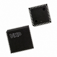
SC16C2552BIA44,512 NXP Semiconductors, SC16C2552BIA44,512 Datasheet - Page 12

SC16C2552BIA44,512
Manufacturer Part Number
SC16C2552BIA44,512
Description
IC UART DUAL SOT187-2
Manufacturer
NXP Semiconductors
Datasheet
1.SC16C2552BIA44529.pdf
(38 pages)
Specifications of SC16C2552BIA44,512
Features
2 Channels
Number Of Channels
2, DUART
Fifo's
16 Byte
Voltage - Supply
2.5V, 3.3V, 5V
With Irda Encoder/decoder
Yes
With False Start Bit Detection
Yes
With Modem Control
Yes
With Cmos
Yes
Mounting Type
Surface Mount
Package / Case
44-LCC (J-Lead)
Lead Free Status / RoHS Status
Lead free / RoHS Compliant
Other names
935274408512
SC16C2552BIA44
SC16C2552BIA44
SC16C2552BIA44
SC16C2552BIA44
NXP Semiconductors
SC16C2552B_3
Product data sheet
7.1 Transmit Holding Register (THR) and Receive Holding Register (RHR)
7.2 Interrupt Enable Register (IER)
The serial transmitter section consists of an 8-bit Transmit Hold Register (THR) and
Transmit Shift Register (TSR). The status of the THR is provided in the Line Status
Register (LSR). Writing to the THR transfers the contents of the data bus (D7 through D0)
to the TSR and UART via the THR, providing that the THR is empty. The THR empty flag
in the LSR[5] register will be set to a logic 1 when the transmitter is empty or when data is
transferred to the TSR.
The serial receive section also contains an 8-bit Receive Holding Register (RHR) and a
Receive Serial Shift Register (RSR). Receive data is removed from the SC16C2552B and
receive FIFO by reading the RHR register. The receive section provides a mechanism to
prevent false starts. On the falling edge of a start or false start bit, an internal receiver
counter starts counting clocks at the 16 clock rate. After 7
should be shifted to the center of the start bit. At this time the start bit is sampled, and if it
is still a logic 0 it is validated. Evaluating the start bit in this manner prevents the receiver
from assembling a false character. Receiver status codes will be posted in the LSR.
The Interrupt Enable Register (IER) masks the interrupts from receiver ready, transmitter
empty, line status and modem status registers. These interrupts would normally be seen
on the INTA, INTB output pins.
Table 7.
Bit
7:4
3
2
1
0
Symbol
IER[7:4]
IER[3]
IER[2]
IER[1]
IER[0]
Interrupt Enable Register bits description
Description
not used; initialized to logic 0
Modem Status Interrupt. This interrupt will be issued whenever there is a
modem status change as reflected in MSR[3:0].
Receive Line Status interrupt. This interrupt will be issued whenever a receive
data error condition exists as reflected in LSR[4:1].
Transmit Holding Register interrupt. In the 16C450 mode, this interrupt will be
issued whenever the THR is empty and is associated with LSR[5]. In the FIFO
modes, this interrupt will be issued whenever the FIFO and THR are empty.
Receive Holding Register. In the 16C450 mode, this interrupt will be issued
when the RHR has data, or is cleared when the RHR is empty. In the FIFO
mode, this interrupt will be issued when the FIFO has reached the
programmed trigger level or is cleared when the FIFO drops below the trigger
level.
5 V, 3.3 V and 2.5 V dual UART, 5 Mbit/s (max.), with 16-byte FIFOs
logic 0 = disable the Modem Status Register interrupt (normal default
condition)
logic 1 = enable the Modem Status Register interrupt
logic 0 = disable the receiver line status interrupt (normal default condition)
logic 1 = enable the receiver line status interrupt
logic 0 = disable the Transmit Holding Register Empty (TXRDY) interrupt
(normal default condition)
logic 1 = enable the TXRDY (ISR level 3) interrupt
logic 0 = disable the receiver ready (ISR level 2, RXRDY) interrupt (normal
default condition)
logic 1 = enable the RXRDY (ISR level 2) interrupt
Rev. 03 — 12 February 2009
1
2
SC16C2552B
clocks, the start bit time
© NXP B.V. 2009. All rights reserved.
12 of 38


