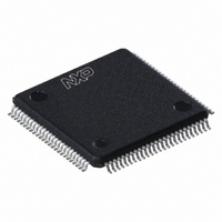
SC28L198A1BE,557 NXP Semiconductors, SC28L198A1BE,557 Datasheet - Page 18

SC28L198A1BE,557
Manufacturer Part Number
SC28L198A1BE,557
Description
IC UART OCTAL W/FIFO 100-LQFP
Manufacturer
NXP Semiconductors
Datasheet
1.SC28L198A1BE557.pdf
(57 pages)
Specifications of SC28L198A1BE,557
Features
False-start Bit Detection
Number Of Channels
8
Fifo's
16 Byte
Voltage - Supply
3.3V, 5V
With Auto Flow Control
Yes
With False Start Bit Detection
Yes
With Modem Control
Yes
With Cmos
Yes
Mounting Type
Surface Mount
Package / Case
100-LQFP
Lead Free Status / RoHS Status
Lead free / RoHS Compliant
Other names
568-1210
935262731557
SC28L198A1BE
935262731557
SC28L198A1BE
Available stocks
Company
Part Number
Manufacturer
Quantity
Price
Company:
Part Number:
SC28L198A1BE,557
Manufacturer:
NXP Semiconductors
Quantity:
10 000
Philips Semiconductors
REGISTER DEFINITIONS
The operation of the Octal UART is programmed by writing control
words into the appropriate registers. Operational feedback is
provided via status registers which can be read by the host CPU.
The Octal UART addressing is loosely divided, by the address bit
A(7), into two parts:
1) That part which is concerned with the configuration of the chip
interface and communication modes.
This part controls the elements of host interface setup, interrupt
arbitration, I/O Port Configuration that part of the UART channel
Table 2. GCCR – Global Configuration Control Register
THIS IS A VERY IMPORTANT REGISTER! IT SHOULD BE THE FIRST REGISTER ADDRESSED DURING INITIALIZATION.
GCCR(7): This bit is reserved for future versions of this device. If
not set to zero most internal addressing will be disabled!
GCCR(6): Bus cycle selection
Controls the operation of the host interface logic. If reset, the power
on/reset default, the host interface can accommodate arbitrarily long
bus I/O cycles. If the bit is set, the Octal UART expects four Sclk
cycle bus I/O operations similar to those produced by an i80386
processor in non–pipelined mode. The major differences in these
modes are observed in the DACKN pin function. In Sync mode, no
negation of CEN is required between cycles.
GCCR(2:1): Interrupt vector configuration
The IVC field controls if and how the assertion of IACKN (the
interrupt acknowledge pin) will form the interrupt vector for the Octal
UART. If b’00, no vector will be presented during an IACKN cycle.
The bus will be driven high (xFF). If the field contains a b’01, the
contents of the IVR, Interrupt Vector Register, will be presented as
the interrupt vector without modification. If IVC = b’10, the channel
code will replace the 3 LSBs of the IVR; if IVC = b’11 then a modified
interrupt type and channel code replace the 5 LSBs of the IVR.
Note: The modified type field IVR(4:3) is:
GCCR(0): Power down control
Controls the power down function. During power down the internal
oscillator is disabled, interrupt arbitration and all data
2006 Aug 10
Bit 7
Reserved
Reserved
Must be set to 0
Octal UART for 3.3 V and 5 V supply voltage
10
11
01
00
Receiver w/o error
Receiver with error
Transmitter
All remaining sources
Bit 6
Sync bus cycles
0 – async cycles
1 – Sync, non–pipe–
lined cycle
Bit 5:3
Reserved
Reserved
Set to 0
Bit 2:1
IVC, Interrupt Vector Control
00 – no interrupt vector
01 – IVR
10 – IVR + channel code
11 – IVR + interrupt type + channel code
18
definitions that do not change in normal data handling. This section
is listed in the ”Register Map, Control”.
2) That part concerned with the transmission and reception of the bit
streams.
This part concerns the data status, FIFO fill levels, data error
conditions, channel status, data flow control (hand shaking). This
section is listed in the ”Register Map, Data”.
The Global Configuration Control Register (GCCR) sets the type of
bus cycle, interrupt vector modification and the power up or down
mode.
transmission/reception activities cease, and all processing for input
change detection, BRG counter/timers and Address/Xon./Xoff
recognition is disabled.
Note: For maximum power savings it is recommended that all
switching inputs be stopped and all input voltage levels be within 0.5
volt of the Vcc and Vss power supply levels.
To switch from the asynchronous to the synchronous bus cycle
mode, a single write operation to the GCCR, terminated by a
negation of the CEN pin, is required. This cycle may be 4 cycles
long if the setup time of the CEN edge to Sclk can be guaranteed.
The host CPU must ensure that a minimum of two Sclk cycles
elapse before the initiation of the next (synchronous) bus cycle(s).
A hardware or software reset is recommended for the unlikely
requirement of returning to the asynchronous bus cycling mode.
MR – Mode Registers
The user must exercise caution when changing the mode of running
receivers, transmitters or BRG counter/timers. The selected mode
will be activated immediately upon selection, even if this occurs
during the reception or transmission of a character. It is also
possible to disrupt internal controllers by changing modes at critical
times, thus rendering later transmission or reception faulty or
impossible. An exception to this policy is switching from auto–echo
or remote loop back modes to normal mode. If the deselection
occurs just after the receiver has sampled the stop bit (in most
cases indicated by the assertion of the channel’s RxRDY bit) and
the transmitter is enabled, the transmitter will remain in auto–echo
mode until the end of the transmission of the stop bit.
Bit 0
Power Down Mode
0 – Device enabled
1 – Power down
SC28L198
Product data sheet


