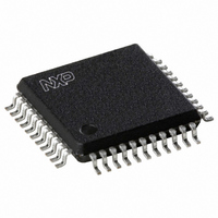
SC28L91A1B,551 NXP Semiconductors, SC28L91A1B,551 Datasheet - Page 13

SC28L91A1B,551
Manufacturer Part Number
SC28L91A1B,551
Description
IC UART SINGLE W/FIFO 44-PQFP
Manufacturer
NXP Semiconductors
Series
IMPACTr
Type
Single Channel UARTr
Datasheet
1.SC28L91A1A529.pdf
(43 pages)
Specifications of SC28L91A1B,551
Number Of Channels
1, UART
Package / Case
44-MQFP, 44-PQFP
Features
False-start Bit Detection
Fifo's
16 Byte
Voltage - Supply
3.3V, 5V
With Auto Flow Control
Yes
With False Start Bit Detection
Yes
With Modem Control
Yes
With Cmos
Yes
Mounting Type
Surface Mount
Data Rate
0.2304 MBd
Supply Voltage (max)
5.5 V
Supply Voltage (min)
3 V
Supply Current
25 mA
Maximum Operating Temperature
+ 85 C
Minimum Operating Temperature
- 40 C
Mounting Style
SMD/SMT
Operating Supply Voltage
3.3 V or 5 V
Lead Free Status / RoHS Status
Lead free / RoHS Compliant
Lead Free Status / RoHS Status
Lead free / RoHS Compliant, Lead free / RoHS Compliant
Other names
568-1187
935267419551
SC28L91A1B-S
935267419551
SC28L91A1B-S
Available stocks
Company
Part Number
Manufacturer
Quantity
Price
Company:
Part Number:
SC28L91A1B,551
Manufacturer:
NXP Semiconductors
Quantity:
10 000
1. Parameters are valid over specified temperature and voltage range.
2. All voltage measurements are referenced to ground (GND). For testing, all inputs swing between 0.4 V and 3.0 V with a transition time of
3. Test conditions for outputs: CL = 125 pF, except open drain outputs. Test conditions for open drain outputs: C
4. Typical values are the average values at +25 C and 5 V.
5. Timing is illustrated and referenced to the WRN and RDN Inputs. Also, CEN may be the “strobing” input. CEN and RDN (also CEN and
6. Guaranteed by characterization of sample units.
7. If CEN is used as the “strobing” input, the parameter defines the minimum High times between one CEN and the next. The RDN signal must
8. Minimum frequencies are not tested but are guaranteed by design.
9. Clocks for 1X mode should maintain a 60/40 duty cycle or better.
10. Minimum DACKN time is t
Philips Semiconductors
NOTES:
NOTES:
2004 Oct 21
Symbol
Receiver Timing, external clock (See Figure 13)
t
t
68000 or Motorola bus timing (See Figures 6, 7, 8)
t
t
t
t
*RXS
*RXH
DCR
DCW
DAT
CSC
3.3 V or 5.0 V Universal Asynchronous
Receiver/Transmitter (UART)
5 ns maximum. For X1/CLK this swing is between 0.4 V and 0.8*V
2.0 V and output voltages of 0.8 V and 2.0 V, as appropriate.
constant current source = 2.6 mA.
WRN) are ORed internally. The signal asserted last initiates the cycle and the signal negated first terminates the cycle.
be negated for t
while in the 68XXX mode. It is not necessary to wait for DACKN to insure the proper operation of the SC28C91. In all cases the data will be
written to the SC28L91 on the falling edge of DACKN or the rise of CEN. The fall of CEN initializes the bus cycle. The rise of CEN ends the
bus cycle. DACKN low or CEN high completes the write cycle.
Bus cycle times:
(ns)
T
dd
(80XXX mode): t
(68XXX mode) = t
60
55
50
45
40
35
30
25
20
15
10
5
0
Parameter
RxD data setup time to RxC high
RxD data hold time from RxC high
DACKN Low (read cycle) from X1 High
DACKN Low (write cycle) from X1 High
DACKN High impedance from CEN or IACKN High
CEN or IACKN setup time to X1 High for minimum DACKN cycle
0
RWD
12 pF
to guarantee that any status register changes are valid.
20
DD
CSC
+ t
30 pF
DCR
RWD
+ t
40
DAT
= t
= 70 ns @ 5V, 40 ns @ 3.3 V + rise and fall time of control signals
Figure 3. Port Timing vs. Capacitive Loading at typical conditions
DSC
+ 1 cycle of the X1 clock @ 5 V + rise and fall time of control signals
+ t
60
DCR
+ two positive edges of the X1 clock. For faster bus cycles, the 80XXX bus timing may be used
80
10
10
100 pF
100
120
pF
125 pF
CC
13
. All time measurements are referenced at input voltages of 0.8 V and
140
160
180
200
Min
50
50
16
SD00684
220
L
Typ
40
40
15
15
8
= 125 pF,
230 pF
Max
35
35
10
240
V
5.0 V @ +25 C
SC28L91
CC
Product data sheet
= 3.3 V @ +25 C
Unit
ns
ns
ns
ns
ns
ns


