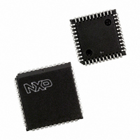
SC16C2552BIA44,529 NXP Semiconductors, SC16C2552BIA44,529 Datasheet - Page 5

SC16C2552BIA44,529
Manufacturer Part Number
SC16C2552BIA44,529
Description
IC UART DUAL W/FIFO 44-PLCC
Manufacturer
NXP Semiconductors
Type
Dual UART with 16-byte FIFOsr
Datasheet
1.SC16C2552BIA44529.pdf
(38 pages)
Specifications of SC16C2552BIA44,529
Number Of Channels
2, DUART
Package / Case
44-LCC (J-Lead)
Features
2 Channels
Fifo's
16 Byte
Voltage - Supply
2.5V, 3.3V, 5V
With Irda Encoder/decoder
Yes
With False Start Bit Detection
Yes
With Modem Control
Yes
With Cmos
Yes
Mounting Type
Surface Mount
Data Rate
5 Mbps
Supply Voltage (max)
5.5 V
Supply Voltage (min)
2.25 V
Supply Current
4.5 mA
Maximum Operating Temperature
+ 85 C
Minimum Operating Temperature
- 40 C
Mounting Style
SMD/SMT
Operating Supply Voltage
2.5 V or 3.3 V or 5 V
Lead Free Status / RoHS Status
Lead free / RoHS Compliant
Lead Free Status / RoHS Status
Lead free / RoHS Compliant, Lead free / RoHS Compliant
Other names
568-3646-5
935274408529
SC16C2552BIA44-S
935274408529
SC16C2552BIA44-S
Available stocks
Company
Part Number
Manufacturer
Quantity
Price
Company:
Part Number:
SC16C2552BIA44,529
Manufacturer:
NXP Semiconductors
Quantity:
10 000
NXP Semiconductors
Table 2.
SC16C2552B_3
Product data sheet
Symbol
RTSA
RTSB
RXA
RXB
TXA
TXB
TXRDYA
TXRDYB
V
XTAL1
XTAL2
CC
Pin description
Pin
36
23
39
25
38
26
1
32
33, 44
11
13
Type
O
O
I
I
O
O
O
O
I
I
O
…continued
Description
Request to Send A, B (active LOW). These outputs are associated with individual UART
channels A through B. A logic 0 on the RTSn pin indicates the transmitter is ready to
transmit data. Writing a logic 1 in the modem control register MCR[1] will set this pin to a
logic 0, indicating that the transmitter is ready to transmit data. After a reset, this pin will be
set to a logic 1.
Receive data A, B. These inputs are associated with individual serial channel data to the
SC16C2552B receive input circuits A through B. The RXn signal will be a logic 1 during
reset, idle (no data). During the local Loopback mode, the RXn input pin is disabled and TXn
data is connected to the UART RXn input, internally.
Transmit data A, B. These outputs are associated with individual serial transmit channel
data from the SC16C2552B. The TXn signal will be a logic 1 during reset, idle (no data), or
when the transmitter is disabled. During the local Loopback mode, the TXn output pin is
disabled and TXn data is internally connected to the UART RXn input.
Transmit Ready A, B (active LOW). These outputs provide the TX FIFO/THR status for
individual transmit channels (A, B). TXRDYn is primarily intended for monitoring
DMA mode 1 transfers for the transmit data FIFOs. An individual channel’s TXRDYA,
TXRDYB buffer ready status is indicated by logic 0, i.e., at least one location is empty and
available in the FIFO or THR. This signal can also be used for single mode transfers (DMA
mode 0).
Power supply input.
Crystal or external clock input. Functions as a crystal input or as an external clock input.
A crystal can be connected between this pin and XTAL2 to form an internal oscillator circuit.
Alternatively, an external clock can be connected to this pin to provide custom data rates.
See
Output of the crystal oscillator or buffered clock. (See also XTAL1.) Crystal oscillator
output or buffered clock output. Should be left open if an external clock is connected to
XTAL1.
Section 6.5 “Programmable baud rate
5 V, 3.3 V and 2.5 V dual UART, 5 Mbit/s (max.), with 16-byte FIFOs
Rev. 03 — 12 February 2009
generator”.
SC16C2552B
© NXP B.V. 2009. All rights reserved.
5 of 38


