SC16C2552BIA44,529 NXP Semiconductors, SC16C2552BIA44,529 Datasheet - Page 4
SC16C2552BIA44,529
Manufacturer Part Number
SC16C2552BIA44,529
Description
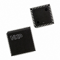
IC UART DUAL W/FIFO 44-PLCC
Manufacturer
NXP Semiconductors
Type
Dual UART with 16-byte FIFOsr
Datasheet
1.SC16C2552BIA44529.pdf
(38 pages)
Specifications of SC16C2552BIA44,529
Number Of Channels
2, DUART
Package / Case
44-LCC (J-Lead)
Features
2 Channels
Fifo's
16 Byte
Voltage - Supply
2.5V, 3.3V, 5V
With Irda Encoder/decoder
Yes
With False Start Bit Detection
Yes
With Modem Control
Yes
With Cmos
Yes
Mounting Type
Surface Mount
Data Rate
5 Mbps
Supply Voltage (max)
5.5 V
Supply Voltage (min)
2.25 V
Supply Current
4.5 mA
Maximum Operating Temperature
+ 85 C
Minimum Operating Temperature
- 40 C
Mounting Style
SMD/SMT
Operating Supply Voltage
2.5 V or 3.3 V or 5 V
Lead Free Status / RoHS Status
Lead free / RoHS Compliant
Lead Free Status / RoHS Status
Lead free / RoHS Compliant, Lead free / RoHS Compliant
Other names
568-3646-5
935274408529
SC16C2552BIA44-S
935274408529
SC16C2552BIA44-S
Available stocks
Company
Part Number
Manufacturer
Quantity
Price
Company:

Part Number:
SC16C2552BIA44,529
Manufacturer:
NXP Semiconductors
Quantity:
10 000


NXP Semiconductors
Table 2.
SC16C2552B_3
Product data sheet
Symbol
D0
D1
D2
D3
D4
D5
D6
D7
DSRA
DSRB
DTRA
DTRB
GND
INTA
INTB
IOR
IOW
MFA
MFB
RESET
RIA
RIB
Pin description
Pin
2
3
4
5
6
7
8
9
41
29
37
27
12, 22
34
17
24
20
35
19
21
43
31
Type
I/O
I/O
I/O
I/O
I/O
I/O
I/O
I/O
I
I
O
O
I
O
O
I
I
O
O
I
I
I
…continued
Description
Data bus (bidirectional). These pins are the 8-bit, 3-state data bus for transferring
information to or from the controlling CPU.
Data Set Ready A, B (active LOW). These inputs are associated with individual UART
channels A through B. A logic 0 on this pin indicates the modem or data set is powered-on
and is ready for data exchange with the UART.
Data Terminal Ready A, B (active LOW). These outputs are associated with individual
UART channels A through B. A logic 0 on this pin indicates that the SC16C2552B is
powered-on and ready. This pin can be controlled via the modem control register. Writing a
logic 1 to MCR[0] will set the DTRn output to logic 0, enabling the modem. This pin will be a
logic 1 after writing a logic 0 to MCR[0], or after a reset.
Signal and power ground.
Interrupt A, B (active HIGH). This function is associated with individual channel interrupts.
Interrupts are enabled in the Interrupt Enable Register (IER). Interrupt conditions include:
receiver errors, available receiver buffer data, transmit buffer empty, or when a modem
status flag is detected.
Read strobe (active LOW). A logic 0 transition on this pin will load the contents of an
internal register defined by address bits A[2:0] onto the SC16C2552B data bus (D[7:0]) for
access by external CPU.
Write strobe (active LOW). A logic 0 transition on this pin will transfer the contents of the
data bus (D[7:0]) from the external CPU to an internal register that is defined by address bits
A[2:0].
Multi-function A, B. This function is associated with an individual channel function, A or B.
User programmable bits 2:1 of the Alternate Function Register (AFR) selects a signal
function or output on these pins. OP2 (interrupt enable), BAUDOUT, and RXRDY are signal
functions that may be selected by the AFR. These signal functions are described as follows:
Reset (active HIGH). A logic 1 on this pin will reset the internal registers and all the outputs.
The UART transmitter output and the receiver input will be disabled during reset time. See
Section 7.11 “SC16C2552B external reset condition”
Ring Indicator A, B (active LOW). These inputs are associated with individual UART
channels A through B. A logic 0 on this pin indicates the modem has received a ringing
signal from the telephone line. A logic 1 transition on this input pin will generate an interrupt
if modem status interrupt is enabled.
OP2. When OP2 is selected, the MFn pin is a logic 0 when MCR[3] is set to a logic 1.
A logic 1 is the default signal condition that is available following a master reset or
power-up.
BAUDOUT. When BAUDOUT function is selected, the 16 baud rate clock output is
available at this pin.
RXRDY. RXRDY is primarily intended for monitoring DMA mode 1 transfers for the receive
data FIFOs. A logic 0 indicates there is receive data to read/unload, i.e., receive ready
status with one or more RX characters available in the FIFO/RHR. This pin is a logic 1
when the FIFO/RHR is empty or when the programmed trigger level has not been
reached. This signal can also be used for single mode transfers (DMA mode 0).
5 V, 3.3 V and 2.5 V dual UART, 5 Mbit/s (max.), with 16-byte FIFOs
Rev. 03 — 12 February 2009
for initialization details.
SC16C2552B
© NXP B.V. 2009. All rights reserved.
4 of 38
Related parts for SC16C2552BIA44,529
Image
Part Number
Description
Manufacturer
Datasheet
Request
R

Part Number:
Description:
Sc16c2552b 5 V, 3.3 V And 2.5 V Dual Uart, 5 Mbit/s Max. , With 16-byte Fifos
Manufacturer:
NXP Semiconductors
Datasheet:
Part Number:
Description:
NXP Semiconductors designed the LPC2420/2460 microcontroller around a 16-bit/32-bitARM7TDMI-S CPU core with real-time debug interfaces that include both JTAG andembedded trace
Manufacturer:
NXP Semiconductors
Datasheet:

Part Number:
Description:
NXP Semiconductors designed the LPC2458 microcontroller around a 16-bit/32-bitARM7TDMI-S CPU core with real-time debug interfaces that include both JTAG andembedded trace
Manufacturer:
NXP Semiconductors
Datasheet:
Part Number:
Description:
NXP Semiconductors designed the LPC2468 microcontroller around a 16-bit/32-bitARM7TDMI-S CPU core with real-time debug interfaces that include both JTAG andembedded trace
Manufacturer:
NXP Semiconductors
Datasheet:
Part Number:
Description:
NXP Semiconductors designed the LPC2470 microcontroller, powered by theARM7TDMI-S core, to be a highly integrated microcontroller for a wide range ofapplications that require advanced communications and high quality graphic displays
Manufacturer:
NXP Semiconductors
Datasheet:
Part Number:
Description:
NXP Semiconductors designed the LPC2478 microcontroller, powered by theARM7TDMI-S core, to be a highly integrated microcontroller for a wide range ofapplications that require advanced communications and high quality graphic displays
Manufacturer:
NXP Semiconductors
Datasheet:
Part Number:
Description:
The Philips Semiconductors XA (eXtended Architecture) family of 16-bit single-chip microcontrollers is powerful enough to easily handle the requirements of high performance embedded applications, yet inexpensive enough to compete in the market for hi
Manufacturer:
NXP Semiconductors
Datasheet:
Part Number:
Description:
The XA-S3 device is a member of Philips Semiconductors? XA(eXtended Architecture) family of high performance 16-bitsingle-chip microcontrollers
Manufacturer:
NXP Semiconductors
Datasheet:

Part Number:
Description:
The NXP BlueStreak LH75401/LH75411 family consists of two low-cost 16/32-bit System-on-Chip (SoC) devices
Manufacturer:
NXP Semiconductors
Datasheet:
Part Number:
Description:
The NXP LPC3130/3131 combine an 180 MHz ARM926EJ-S CPU core, high-speed USB2
Manufacturer:
NXP Semiconductors
Datasheet:
Part Number:
Description:
The NXP LPC3141 combine a 270 MHz ARM926EJ-S CPU core, High-speed USB 2
Manufacturer:
NXP Semiconductors
Part Number:
Description:
The NXP LPC3143 combine a 270 MHz ARM926EJ-S CPU core, High-speed USB 2
Manufacturer:
NXP Semiconductors

Part Number:
Description:
The NXP LPC3152 combines an 180 MHz ARM926EJ-S CPU core, High-speed USB 2
Manufacturer:
NXP Semiconductors
Part Number:
Description:
The NXP LPC3154 combines an 180 MHz ARM926EJ-S CPU core, High-speed USB 2
Manufacturer:
NXP Semiconductors