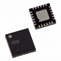
SC16IS760IBS,151 NXP Semiconductors, SC16IS760IBS,151 Datasheet - Page 33

SC16IS760IBS,151
Manufacturer Part Number
SC16IS760IBS,151
Description
IC UART I2C/SPI 24-HVQFN
Manufacturer
NXP Semiconductors
Type
IrDA or RS- 232 or RS- 485r
Datasheet
1.SC16IS740IPW112.pdf
(62 pages)
Specifications of SC16IS760IBS,151
Number Of Channels
1, UART
Package / Case
24-VQFN Exposed Pad, 24-HVQFN, 24-SQFN, 24-DHVQFN
Features
Low Current
Fifo's
64 Byte
Protocol
RS232, RS485
Voltage - Supply
2.5V, 3.3V, 5V
With Auto Flow Control
Yes
With False Start Bit Detection
Yes
With Modem Control
Yes
Mounting Type
Surface Mount
Data Rate
5 Mbps
Supply Voltage (max)
3.6 V
Supply Voltage (min)
2.3 V
Supply Current
6 mA
Maximum Operating Temperature
+ 85 C
Minimum Operating Temperature
- 40 C
Mounting Style
SMD/SMT
Operating Supply Voltage
2.5 V or 3.3 V
Lead Free Status / RoHS Status
Lead free / RoHS Compliant
For Use With
568-4000 - DEMO BOARD SPI/I2C TO DUAL UART568-3510 - DEMO BOARD SPI/I2C TO UART
Lead Free Status / Rohs Status
Lead free / RoHS Compliant
Other names
568-2238
935279279151
SC16IS760IBS-S
935279279151
SC16IS760IBS-S
NXP Semiconductors
SC16IS740_750_760_6
Product data sheet
8.15 Receiver FIFO Level register (RXLVL)
8.16 Programmable I/O pins Direction register (IODir)
8.17 Programmable I/O pins State Register (IOState)
8.18 I/O Interrupt Enable Register (IOIntEna)
This register is a read-only register, it reports the fill level of the receive FIFO. That is, the
number of characters in the RX FIFO.
Table 26.
This register is only available on the SC16IS750 and SC16IS760. This register is used to
program the I/O pins direction. Bit 0 to bit 7 controls GPIO0 to GPIO7.
Table 27.
Remark: If there is a pending input (GPIO) interrupt and IODir is written, this pending
interrupt will be cleared, that is, the interrupt signal will be negated.
This register is only available on the SC16IS750 and SC16IS760. When ‘read’, this
register returns the actual state of all I/O pins. When ‘write’, each register bit will be
transferred to the corresponding IO pin programmed as output.
Table 28.
This register is only available on the SC16IS750 and SC16IS760. This register enables
the interrupt due to a change in the I/O configured as inputs. If GPIO[7:4] are programmed
as modem pins, their interrupt generation must be enabled via IER register bit 3. In this
case bit 7 to bit 4 of IOIntEna will have no effect on GPIO[7:4].
Table 29.
Bit
7
6:0
Bit
7:0
Bit
7:0
Bit
7:0
Symbol
-
RXLVL[6:0]
Symbol
IODir
Symbol
IOState
Symbol
IOIntEna
Receiver FIFO Level register bits description
IODir register bits description
IOState register bits description
IOIntEna register bits description
Single UART with I
Rev. 06 — 13 May 2008
Description
not used; set to zeros
number of characters stored in RX FIFO, from 0 (0x00) to 64 (0x40)
Description
set GPIO pins [7:0] to input or output
Description
Write this register:
Read this register:
Description
input interrupt enable
0 = input
1 = output
set the logic level on the output pins
return states of all pins
0 = a change in the input pin will not generate an interrupt
1 = a change in the input will generate an interrupt
0 = set output pin to zero
1 = set output pin to one
2
C-bus/SPI interface, 64-byte FIFOs, IrDA SIR
SC16IS740/750/760
© NXP B.V. 2008. All rights reserved.
33 of 62


