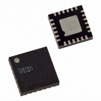
SC16IS760IBS,151 NXP Semiconductors, SC16IS760IBS,151 Datasheet - Page 23

SC16IS760IBS,151
Manufacturer Part Number
SC16IS760IBS,151
Description
IC UART I2C/SPI 24-HVQFN
Manufacturer
NXP Semiconductors
Type
IrDA or RS- 232 or RS- 485r
Datasheet
1.SC16IS740IPW112.pdf
(62 pages)
Specifications of SC16IS760IBS,151
Number Of Channels
1, UART
Package / Case
24-VQFN Exposed Pad, 24-HVQFN, 24-SQFN, 24-DHVQFN
Features
Low Current
Fifo's
64 Byte
Protocol
RS232, RS485
Voltage - Supply
2.5V, 3.3V, 5V
With Auto Flow Control
Yes
With False Start Bit Detection
Yes
With Modem Control
Yes
Mounting Type
Surface Mount
Data Rate
5 Mbps
Supply Voltage (max)
3.6 V
Supply Voltage (min)
2.3 V
Supply Current
6 mA
Maximum Operating Temperature
+ 85 C
Minimum Operating Temperature
- 40 C
Mounting Style
SMD/SMT
Operating Supply Voltage
2.5 V or 3.3 V
Lead Free Status / RoHS Status
Lead free / RoHS Compliant
For Use With
568-4000 - DEMO BOARD SPI/I2C TO DUAL UART568-3510 - DEMO BOARD SPI/I2C TO UART
Lead Free Status / Rohs Status
Lead free / RoHS Compliant
Other names
568-2238
935279279151
SC16IS760IBS-S
935279279151
SC16IS760IBS-S
NXP Semiconductors
SC16IS740_750_760_6
Product data sheet
8.1 Receive Holding Register (RHR)
8.2 Transmit Holding Register (THR)
8.3 FIFO Control Register (FCR)
The receiver section consists of the Receiver Holding Register (RHR) and the Receiver
Shift Register (RSR). The RHR is actually a 64-byte FIFO. The RSR receives serial data
from the RX pin. The data is converted to parallel data and moved to the RHR. The
receiver section is controlled by the Line Control Register. If the FIFO is disabled, location
zero of the FIFO is used to store the characters.
The transmitter section consists of the Transmit Holding Register (THR) and the Transmit
Shift Register (TSR). The THR is actually a 64-byte FIFO. The THR receives data and
shifts it into the TSR, where it is converted to serial data and moved out on the TX pin. If
the FIFO is disabled, the FIFO is still used to store the byte. Characters are lost if overflow
occurs.
This is a write-only register that is used for enabling the FIFOs, clearing the FIFOs, setting
transmitter and receiver trigger levels.
Table 11.
Bit
7:6
5:4
3
2
1
0
Symbol
FCR[7] (MSB),
FCR[6] (LSB)
FCR[5] (MSB),
FCR[4] (LSB)
FCR[3]
FCR[2]
FCR[1]
FCR[0]
FIFO Control Register bits description
[1]
[1]
Description
RX trigger. Sets the trigger level for the RX FIFO.
TX trigger. Sets the trigger level for the TX FIFO.
FCR[5:4] can only be modified and enabled when EFR[4] is set. This is
because the transmit trigger level is regarded as an enhanced function.
reserved
reset TX FIFO
reset RX FIFO
FIFO enable
Single UART with I
00 = 8 characters
01 = 16 characters
10 = 56 characters
11 = 60 characters
00 = 8 spaces
01 = 16 spaces
10 = 32 spaces
11 = 56 spaces
logic 0 = no FIFO transmit reset (normal default condition)
logic 1 = clears the contents of the transmit FIFO and resets the FIFO
level logic (the Transmit Shift Register is not cleared or altered). This bit
will return to a logic 0 after clearing the FIFO.
logic 0 = no FIFO receive reset (normal default condition)
logic 1 = clears the contents of the receive FIFO and resets the FIFO
level logic (the Receive Shift Register is not cleared or altered). This bit
will return to a logic 0 after clearing the FIFO.
logic 0 = disable the transmit and receive FIFO (normal default condition)
logic 1 = enable the transmit and receive FIFO
Rev. 06 — 13 May 2008
Table 11
2
C-bus/SPI interface, 64-byte FIFOs, IrDA SIR
shows FIFO Control Register bit settings.
SC16IS740/750/760
© NXP B.V. 2008. All rights reserved.
23 of 62


