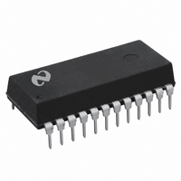
TP11362AN National Semiconductor, TP11362AN Datasheet - Page 8

TP11362AN
Manufacturer Part Number
TP11362AN
Description
IC PROCESSOR QUAD DIFF PCM 24DIP
Manufacturer
National Semiconductor
Datasheet
1.TP11362AN.pdf
(16 pages)
Specifications of TP11362AN
Function
Adaptive Differential Pulse Code Modulation (ADPCM) Transcoder
Interface
PCM, Serial
Number Of Circuits
4
Voltage - Supply
5V
Current - Supply
7mA
Power (watts)
35mW
Operating Temperature
-40°C ~ 85°C
Mounting Type
Through Hole
Package / Case
*
Lead Free Status / RoHS Status
Contains lead / RoHS non-compliant
Other names
*TP11362AN
www.national.com
Note 1: x = Don’t Care state
Note 2: x = unknown (but defined) state
Note 3: x = unknown (but defined) state
Functional Description
to the falling edge of CE are latched in. In Table 3 , the last in-
put bit prior to to the CE falling edge is the LSB of the AD-
PCM data word.
Note that the serial input data is referenced to the falling
edge of CE while the serial output data is referenced to the
rising edge of CE. TSI and RSI input data are clocked in with
the false edge of PSCK and ASCK, respectively. The MSB of
TSO and RSO output data are shifted out with the falling
SINGLE-CHANNEL INITIALIZATION AND
ALL-CHANNEL RESET
The TP11362A ADPCM processor can be initialized on a
per-channel basis via the use of INIT or on an all-channel ba-
sis via the use of RSTB. In both cases, the internal ADPCM
variables are initialized to the default values as suggested by
the ITU G.726 recommendation.
An individual channel can be initialized to the desired con-
figuration by setting the corresponding data variables PCM1,
EN, QSEL(0,1) and by asserting the INIT pin high. The con-
figuration data and INIT signal are strobed at the falling edge
of CE. For an initialization cycle, the period of CE must be 45
master clock (CLK) cycles. The transcoder is then ready to
process the next channel.
The active low RSTB signal is used for a “warm” reset as
well as for facilitating device testing. The initialization of the
QSEL1
QSEL1
QSEL1
0
0
1
1
0
0
1
1
0
0
1
1
QSEL0
0
1
0
1
while CE is High (the First Bit is the MSB Data Bit following the Rising Edge of CE)
QSEL0
QSEL0
TABLE 4. Transfer Order of ADPCM Output Data (TSO) with 4 ASCK Rising Edges
0
1
0
1
0
1
0
1
32 kbps
24 kbps
16 kbps
40 kbps
TABLE 3. Transfer Order of ADPCM Input Data (RSI). The Last Bit Prior
Mode
with 7 ASCK Rising Edges (8 Low Pulses) of ASCK while CE is High
to the Falling Edge of CE is the LSB of the ADPCM Data
TABLE 5. Transfer Order of ADPCM Output Data (TSO)
32 kbps
24 kbps
16 kbps
40 kbps
32 kbps
24 kbps
16 kbps
40 kbps
Mode
Mode
Bit 8
(Continued)
D3
D2
D1
D4
Bit 7
D2
D1
D0
D3
(MSB)
(MSB)
Bit 5
Bit 5
D4
D3
D2
D1
D4
x
x
x
Bit 6
D1
D0
D2
8
x
edge of CE. Subsequent TSO and RSO data are shifted out
with the rising edges of ASCK and PSCK respectively.
Table 4 shows the transfer order of the ADPCM output data.
In the case where there are more ASCK clocks than the
ADPCM data, the ADPCM output will recirculate.
For example, if the 32 kbps mode is selected, and eight low
pulses of ASCK exist within the CE high pulse, the following
ADPCM encoded data D3-D2-D1-D0-D3-D2-D1-D0 will ap-
pear at the TSO output ( Table 5 ).
internal memory takes 726 CLK cycles after the RSTB goes
inactive (logic “1”). The first transition of CE is allowed six
CLK cycles after RSTB goes inactive. It is recommended
that CE be kept low during the initialization phase.The rec-
ommended values for ASCK and PSCK during initialization
are logic “1”, and that for TSI and RSI logic “0”. Any data (TSI
and RSI) applied during the initialization phase will be lost,
however, they won’t affect the proper initialization process-
.The minimum low time of RSTB is 2 CLK cycles.
The chip resumes operation on the first negative edge of CE
after the completion of the initialization.
POWER-ON-RESET
The on-chip Power-On-Reset macro is activated when exter-
nal power is first applied to the device. It has the same func-
tion as the external RSTB pin which initializes all channels to
the default values defined in the ITU Recommendation
Bit 4
Bit 4
D3
D2
D1
D3
D2
D1
D0
D3
Bit 5
D0
D1
x
x
Bit 4
Bit 3
Bit 3
D3
D2
D1
D0
D2
D1
D0
D2
D1
D0
D2
x
Bit 3
D2
D1
D0
D4
Bit 2
Bit 2
D1
D0
D1
D0
D1
x
x
x
Bit 2
D1
D0
D3
x
(LSB)
(LSB)
Bit 1
Bit 1
D0
D0
D3
D2
D1
D0
x
x
Bit 1
D0
D2
x
x


