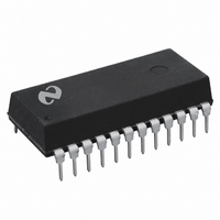
TP11362AN National Semiconductor, TP11362AN Datasheet - Page 4

TP11362AN
Manufacturer Part Number
TP11362AN
Description
IC PROCESSOR QUAD DIFF PCM 24DIP
Manufacturer
National Semiconductor
Datasheet
1.TP11362AN.pdf
(16 pages)
Specifications of TP11362AN
Function
Adaptive Differential Pulse Code Modulation (ADPCM) Transcoder
Interface
PCM, Serial
Number Of Circuits
4
Voltage - Supply
5V
Current - Supply
7mA
Power (watts)
35mW
Operating Temperature
-40°C ~ 85°C
Mounting Type
Through Hole
Package / Case
*
Lead Free Status / RoHS Status
Contains lead / RoHS non-compliant
Other names
*TP11362AN
www.national.com
Functional Description
The TP11362A is capable of processing eight independent
channels (half duplex) or four full-duplex PCM channels
within 125 µs (8 kHz).
The logic state of TRB at the falling edge of CE determines
which input register is active during that CE period and which
output register will be active in the following third CE period.
The input data is processed (PCM data encoded or ADPCM
data decoded) during the second cycle and shifted out in the
third cycle of CE while CE is high.
SERIAL I/O
Input data is transferred into the TP11362A on the falling
edge of the clock signal, while output data is transmitted on
the rising edge of the clock signal. PCM data is transferred
synchronously using PSCK, while ADPCM data is trans-
ferred synchronously using ASCK. The clock signals ASCK
and PSCK should be high while CE changes. All serial data
is transferred with MSB first. Figure 2 and Figure 3 show the
serial input and output structures, respectively.
PCM Serial Input Register
The serial PCM data to be encoded is shifted into the 8-bit
PCM input register with the falling edges of PSCK while CE
and TRB are high. The falling edge of CE latches the state of
ADPCM Output Register
The internal encoded parallel ADPCM data is loaded into the
5-bit ADPCM output register with the falling edge of CE sig-
nal. The first MSB data is shifted out after the rising edge of
CE, subsequent ADPCM serial data is shifted out with the
rising edge of ASCK. Table 4 shows the transfer order of the
ADPCM output data. If more than 4 ASCK clocks are avail-
able while CE is high in the 32, 24, and 16 kbps modes, the
ADPCM output data will recirculate starting with the MSB. In
the case of the 40 kbps mode, the ADPCM output pattern will
recirculate, starting with the MSB, with the fifth rising edge of
ASCK while CE is high.
(Continued)
FIGURE 2. Serial Input Structure
4
the input register and transfers the last 8 bits data prior to the
CE transition to the core for processing. The 8-bit PCM input
register is cleared asynchronously with RSTB going low.
ADPCM Serial Input Register
The ADPCM serial input register is a 5-bit shift register to
store the 5-bit data in the 40 kbps ADPCM mode. Serial input
data is latched in with the falling edges of ASCK while CE is
high and TRB is low. A minimum number of five low going
ASCK pulses must be available within the CE pulse when
operating in the 40 kbps mode. For the 32, 24 and 16 kbps
modes, ASCK must be pulsed low 4 times while CE is high to
read in the RSI data. The falling edge of CE latches the last
5 bits data in the 40 kbps mode or the last 4 bits data in the
32, 24, and 16 kbps modes prior to the CE transistion. See
Table 3 for the position of the ADPCM data in the 5-bit input
register when 5 ASCK low going pulses occur while CE is
high and TRB is low. Bit 1 in Table 3 is the LSB which is the
last bit in 32 and 40 kbps modes referenced to the negative
edge of CE.
PCM Output Register
The decoded 8-bit parallel PCM data is loaded into an 8-bit
parallel-to-serial output shift register with the falling edge of
CE. The MSB data is shifted out with the leading edge of CE,
and subsequent data are shifted out with the rising edges of
PSCK while CE is high. The 8-bit PCM data at the RSO out-
put will recirculate with the MSB first after the seventh rising
edge of PSCK while CE is high.
Figure 4 shows the full duplex timing diagram for the 40 kbps
mode. For the 32, 24 and 16 kbps modes only four ASCK low
pulses are needed while CE is high.
TRB is alternate high and low in the full duplex mode at each
falling edge of CE for a transmit (encoder) operation followed
DS012877-4


