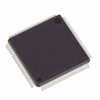
DS21352L Maxim Integrated Products, DS21352L Datasheet - Page 43

DS21352L
Manufacturer Part Number
DS21352L
Description
IC TXRX T1 1-CHIP 3.3V 100-LQFP
Manufacturer
Maxim Integrated Products
Datasheet
1.DS21352L.pdf
(137 pages)
Specifications of DS21352L
Function
Single-Chip Transceiver
Interface
HDLC, T1
Number Of Circuits
1
Voltage - Supply
3.14 V ~ 3.47 V
Current - Supply
75mA
Operating Temperature
0°C ~ 70°C
Mounting Type
Surface Mount
Package / Case
100-LQFP
Includes
DSX-1 and CSU Line Build-Out Generator, HDLC Controller, In-Band Loop Code Generator and Detector
Lead Free Status / RoHS Status
Contains lead / RoHS non-compliant
Power (watts)
-
Available stocks
Company
Part Number
Manufacturer
Quantity
Price
Company:
Part Number:
DS21352L
Manufacturer:
JRC
Quantity:
5 510
Part Number:
DS21352L
Manufacturer:
DALLAS
Quantity:
20 000
Company:
Part Number:
DS21352LN+
Manufacturer:
Maxim Integrated Products
Quantity:
135
DS21352/DS21552
7. STATUS AND INFORMATION REGISTERS
There is a set of nine registers that contain information on the current real time status of the device, Status
Register 1 (SR1), Status Register 2 (SR2), Receive Information Registers 1 to 3 (RIR1/RIR2/RIR3) and a
set of four registers for the onboard HDLC and BOC controller. The specific details on the four registers
pertaining to the HDLC controller are covered in Section 15.3.2 but they operate the same as the other
status registers in the DS21352/552 and this operation is described below.
When a particular event has occurred (or is occurring), the appropriate bit in one of these nine registers
will be set to a one. All of the bits in SR1, SR2, RIR1, RIR2, and RIR3 registers operate in a latched
fashion. This means that if an event or an alarm occurs and a bit is set to a one in any of the registers, it
will remain set until the user reads that bit. The bit will be cleared when it is read and it will not be set
again until the event has occurred again (or in the case of the RBL, RYEL, LRCL, and RLOS alarms, the
bit will remain set if the alarm is still present). There are bits in the four HDLC status registers that are
not latched and these bits are listed in Section 15.3.2.
The user will always proceed a read of any of the nine registers with a write. The byte written to the
register will inform the DS21352/552 which bits the user wishes to read and have cleared. The user will
write a byte to one of these registers, with a one in the bit positions he or she wishes to read and a zero in
the bit positions he or she does not wish to obtain the latest information on. When a one is written to a bit
location, the read register will be updated with the latest information. When a zero is written to a bit
position, the read register will not be updated and the previous value will be held. A write to the status
and information registers will be immediately followed by a read of the same register. The read result
should be logically AND’ed with the mask byte that was just written and this value should be written
back into the same register to insure that bit does indeed clear. This second write step is necessary
because the alarms and events in the status registers occur asynchronously in respect to their access via
the parallel port. This write–read– write scheme allows an external microcontroller or microprocessor to
individually poll certain bits without disturbing the other bits in the register. This operation is key in
controlling the DS21352/552 with higher–order software languages.
The SR1, SR2, and HSR registers have the unique ability to initiate a hardware interrupt via the INT
output pin. Each of the alarms and events in the SR1, SR2, and HSR can be either masked or unmasked
from the interrupt pin via the Interrupt Mask Register 1 (IMR1), Interrupt Mask Register 2 (IMR2), and
HDLC Interrupt Mask Register (HIMR) respectively. The HIMR register is covered in Section 15.3.2.
The interrupts caused by alarms in SR1 (namely RYEL, LRCL, RBL, and RLOS) act differently than the
interrupts caused by events in SR1 and SR2 (namely LUP, LDN, LOTC, RSLIP, RMF, TMF, SEC,
RFDL, TFDL, RMTCH, RAF, and RSC) and HIMR. The alarm caused interrupts will force the INT pin
low whenever the alarm changes state (i.e., the alarm goes active or inactive according to the set/clear
criteria in Table 7-2). The INT pin will be allowed to return high (if no other interrupts are present) when
the user reads the alarm bit that caused the interrupt to occur even if the alarm is still present. The event
caused interrupts will force the INT pin low when the event occurs. The INT pin will be allowed to return
high (if no other interrupts are present) when the user reads the event bit that caused the interrupt to
occur.
43 of 137


