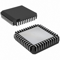
DS2153Q-A7+T&R Maxim Integrated Products, DS2153Q-A7+T&R Datasheet - Page 12

DS2153Q-A7+T&R
Manufacturer Part Number
DS2153Q-A7+T&R
Description
IC TXRX E1 1-CHIP 5V 44-PLCC
Manufacturer
Maxim Integrated Products
Datasheet
1.DS2153Q-A7TR.pdf
(60 pages)
Specifications of DS2153Q-A7+T&R
Function
Single-Chip Transceiver
Interface
E1
Number Of Circuits
1
Voltage - Supply
4.75 V ~ 5.25 V
Current - Supply
65mA
Operating Temperature
0°C ~ 70°C
Mounting Type
Surface Mount
Package / Case
*
Lead Free Status / RoHS Status
Lead free / RoHS Compliant
Power (watts)
-
TCR1: TRANSMIT CONTROL REGISTER 1 (Address = 12 Hex)
Note: For details about how the Transmit Control Registers affect the operation of the DS2153Q, see
Figure
(MSB)
SYMBOL
TUA1
—
TFPT
TSA1
TSIO
T16S
TSM
TSiS
—
14-9.
TFPT
POSITION
TCR1.7
TCR1.6
TCR1.5
TCR1.4
TCR1.3
TCR1.2
TCR1.1
TCR1.0
T16S
NAME AND DESCRIPTION
Not Assigned. Should be set to 0 when written to.
Transmit Time Slot 0 Pass Through.
0 = FAS bits/Sa bits/Remote Alarm sourced internally from the
TAF and TNAF registers
1 = FAS bits/Sa bits/Remote Alarm sourced from TSER
Transmit Time Slot 16 Data Select.
0 = sample time slot 16 at TSER pin
1 = source time slot 16 from TS1 to TS16 registers
Transmit Unframed All Ones.
0 = transmit data normally
1 = transmit an unframed all ones code at TPOS and TNEG
Transmit International Bit Select.
0 = sample Si bits at TSER pin
1 = source Si bits from TAF and TNAF registers (in this mode,
TCR1.6 must be set to 0)
Transmit Signaling All Ones.
0 = normal operation
1 = force time slot 16 in every frame to all ones
TSYNC Mode Select.
0 = frame mode (see the timing in Section 14)
1 = CAS and CRC4 multiframe mode (see the timing in Section 14)
TSYNC I/O Select.
0 = TSYNC is an input
1 = TSYNC is an output
TUA1
12 of 60
TSiS
TSA1
TSM
TSIO
(LSB)


