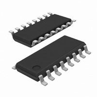
SI3019-F-GSR Silicon Laboratories Inc, SI3019-F-GSR Datasheet - Page 86

SI3019-F-GSR
Manufacturer Part Number
SI3019-F-GSR
Description
IC VOICE DAA GCI/PCM/SPI 16SOIC
Manufacturer
Silicon Laboratories Inc
Datasheet
1.SI3019-F-GSR.pdf
(112 pages)
Specifications of SI3019-F-GSR
Function
Data Access Arrangement (DAA)
Interface
GCI, PCM, SPI
Number Of Circuits
1
Voltage - Supply
3 V ~ 3.6 V
Current - Supply
8.5mA
Operating Temperature
-40°C ~ 85°C
Mounting Type
Surface Mount
Package / Case
16-SOIC (3.9mm Width)
Includes
Line Voltage Monitor, Loop Current Monitor, Overload Detection, Parallel Handset Detection, Polarity Reversal Detection, TIP and
Lead Free Status / RoHS Status
Lead free / RoHS Compliant
Power (watts)
-
Lead Free Status / RoHS Status
Supplier Unconfirmed, Lead free / RoHS Compliant
- Current page: 86 of 112
- Download datasheet (2Mb)
Si3050 + Si3018/19
Register 37. PCM Receive Start Count—High Byte
Reset settings = 0000_0000
Register 38. TX Gain Control 2
Reset settings = 0000_0000
86
Bit
7:2
1:0
Bit
7:5
3:0
4
Name
Name
Type
Type
Bit
Bit
TXG2[3:0] Transmit Gain 2.
Reserved Read returns zero.
Reserved
Name
RXS[1:0]
TGA2
Name
D7
D7
Transmit Gain or Attenuation 2.
0 = Incrementing the TXG2[3:0] bits results in gaining up the transmit path.
1 = Incrementing the TXG2[3:0] bits results in attenuating the transmit path.
Each bit increment represents 1 dB of gain or attenuation, up to a maximum of +12 dB and
–15 dB respectively.
For example:
TGA2
X
0
0
0
1
1
1
PCM Receive Start Count.
PCM Receive Start Count equals the number of PCLKs following FSYNC before data
reception begins.
Read returns zero.
D6
D6
TXG2[3:0]
0000
0001
11xx
0001
1111
:
:
D5
D5
Rev. 1.31
0 dB gain or attenuation is applied to the transmit path.
1 dB gain is applied to the transmit path.
12 dB gain is applied to the transmit path.
1 dB attenuation is applied to the transmit path.
15 dB attenuation is applied to the transmit path.
Result
TGA2
R/W
D4
D4
Function
Function
D3
D3
D2
D2
TXG2[3:0]
R/W
D1
D1
RXS[1:0]
R/W
D0
D0
Related parts for SI3019-F-GSR
Image
Part Number
Description
Manufacturer
Datasheet
Request
R
Part Number:
Description:
IC VOICE DAA GCI/PCM/SPI 16TSSOP
Manufacturer:
Silicon Laboratories Inc
Datasheet:

Part Number:
Description:
IC VOICE DAA GCI/PCM/SPI 16SOIC
Manufacturer:
Silicon Laboratories Inc
Datasheet:

Part Number:
Description:
IC VOICE DAA GCI/PCM/SPI 16SOIC
Manufacturer:
Silicon Laboratories Inc
Datasheet:
Part Number:
Description:
Manufacturer:
Silicon Laboratories Inc
Datasheet:
Part Number:
Description:
IC VOICE DAA GCI/PCM/SPI 20-QFN
Manufacturer:
Silicon Laboratories Inc
Datasheet:
Part Number:
Description:
Modem Chip Chipset 16-Pin SOIC T/R
Manufacturer:
Silicon Laboratories Inc

Part Number:
Description:
IC VOICE DAA GCI/PCM/SPI 16SOIC
Manufacturer:
Silicon Laboratories Inc
Part Number:
Description:
Telecom Line Management ICs Si3050 Enhncd Global Voice DAA Line-Side
Manufacturer:
Silicon Laboratories Inc
Part Number:
Description:
Telecom Line Management ICs Si3050 Enhanced Glo Voice DAA Line-Side
Manufacturer:
Silicon Laboratories Inc
Part Number:
Description:
Manufacturer:
Silicon Laboratories Inc
Datasheet:
Part Number:
Description:
IC VOICE DAA GCI/PCM/SPI 16TSSOP
Manufacturer:
Silicon Laboratories Inc
Datasheet:

Part Number:
Description:
IC VOICE DAA GCI/PCM/SPI 16SOIC
Manufacturer:
Silicon Laboratories Inc
Datasheet:


