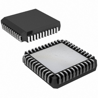
DS2151QB+ Maxim Integrated Products, DS2151QB+ Datasheet - Page 32

DS2151QB+
Manufacturer Part Number
DS2151QB+
Description
IC TXRX T1 1-CHIP 5V LP 44-PLCC
Manufacturer
Maxim Integrated Products
Datasheet
1.DS2151QB.pdf
(60 pages)
Specifications of DS2151QB+
Function
Single-Chip Transceiver
Interface
T1
Number Of Circuits
1
Voltage - Supply
4.75 V ~ 5.25 V
Current - Supply
65mA
Operating Temperature
0°C ~ 70°C
Mounting Type
Surface Mount
Package / Case
44-LCC, 44-PLCC
Includes
Alarm Detector and Generator, CSU Loop Codes Generator and Detector, DSX-1 and CSU Line Build-Outs Generator
Lead Free Status / RoHS Status
Lead free / RoHS Compliant
Power (watts)
-
8 SIGNALING OPERATION
The Robbed-Bit signaling bits embedded in the T1 stream can be extracted from the receive stream and
inserted into the transmit stream by the DS2151Q. There is a set of 12 registers for the receive side (RS1
to RS12) and 12 registers on the transmit side (TS1 to TS12). The signaling registers are detailed below.
The CCR1.5 bit is used to control the robbed signaling bits as they appear at RSER. If CCR1.5 is set to 0,
then the robbed signaling bits will appear at RSER in their proper position as they are received. If
CCR1.5 is set to a 1, then the robbed signaling bit positions will be forced to a 1 at RSER.
RS1 TO RS12: RECEIVE SIGNALING REGISTERS (Address = 60 to 6B Hex)
Each Receive Signaling Register (RS1 to RS12) reports the incoming Robbed-Bit signaling from eight
DS0 channels. In the ESF framing mode, there can be up to 4 signaling bits per channel (A, B, C, and D).
In the D4 framing mode, there are only 2 framing bits per channel (A and B). In the D4 framing mode,
the DS2151Q will replace the C and D signaling bit positions with the A and B signaling bits from the
previous multiframe. Hence, whether the DS2151Q is operated in either framing mode, the user needs
only to retrieve the signaling bits every 3ms. The bits in the Receive Signaling Registers are updated on
multiframe boundaries so the user can utilize the Receive Multiframe Interrupt in the Receive Status
Register 2 (SR2.7) to know when to retrieve the signaling bits. The Receive Signaling Registers are
frozen and not updated during a loss of sync condition (SR1.0 = 1). They will contain the most recent
signaling information before the “OOF” occurred.
A/C(16)
A/C(24)
B/D(16)
B/D(24)
(MSB)
A/C(8)
B/D(8)
A(16)
A(24)
B(16)
B(24)
A(8)
B(8)
SYMBOL
D(24)
A(1)
A/C(15)
A/C(23)
B/D(15)
B/D(23)
A/C(7)
B/D(7)
A(15)
A(23)
B(15)
B(23)
A(7)
B(7)
A/C(14)
A/C(22)
B/D(14)
B/D(22)
A/C(6)
B/D(6)
A(14)
A(22)
B(14)
B(22)
A(6)
B(6)
POSITION
RS12.7
RS1.0
A/C(13)
B/D(13)
B/D(21)
A/C(5)
A/C(1)
B/D(5)
A(13)
A(21)
B(13)
B(21)
A(5)
B(5)
A/C(12)
A/C(20)
B/D(12)
B/D(20)
NAME AND DESCRIPTION
Signaling Bit D in Channel 24
Signaling Bit A in Channel 1
A/C(4)
B/D(4)
A(12)
A(20)
B(12)
B(20)
A(4)
B(4)
32 of 60
A/C(11)
A/C(19)
B/D(11)
B/D(19)
A/C(3)
B/D(3)
A(11)
A(19)
B(11)
B(19)
A(3)
B(3)
A/C(10)
A/C(18)
B/D(10)
B/D(18)
A/C(2)
B/D(2)
A(10)
A(18)
B(10)
B(18)
A(2)
B(2)
A/C(17)
B/D(17)
A/C(1)
A/C(9)
B/D(1)
B/D(9)
(LSB)
A(17)
B(17)
A(1)
A(9)
B(1)
B(9)
RS11 (6A)
RS12 (6B)
RS10 (69)
RS1 (60)
RS2 (61)
RS3 (62)
RS4 (63)
RS5 (64)
RS6 (65)
RS7 (66)
RS8 (67)
RS9 (68)


